


Selenide Compounds
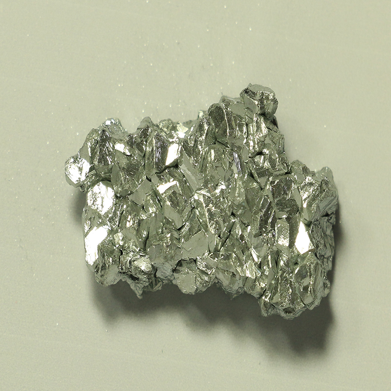
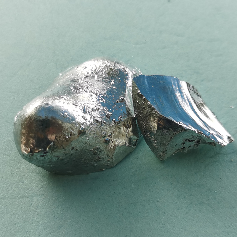
Antimony Selenide Sb2Se3 is a economic, non-toxicity and stable inorganic thin film solar cell material. Antimony Selenide Sb2Se3 crystal exhibits topological insulator state, superconductivity, high thermoelectric efficiency, ideal environmental stability and high crystalline order, which has applications in thermoelectric, photovoltaic and optical storage. Sb2Se3 photodetectors show excellent photoelectric performance, mid-infrared frequency conversion, and nonlinear applications. Selenide compound find many application as electrolyte material, semiconductor dopant, QLED display, IC field and other material fields etc.
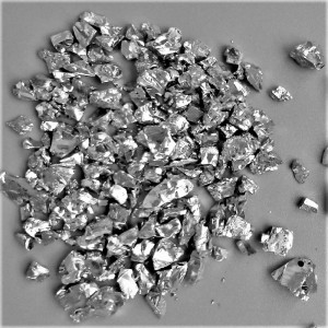
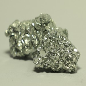
Selenide Compounds mainly refer to the metal elements and metalloid compounds, which have stoichiometric composition changing within a certain range to form a compound-based solid solution. Inter-metallic compound is of its excellent properties between the metal and ceramic, and become an important branch of the new structural materials. Selenide compound of Antimony Selenide Sb2Se3, Arsenic Selenide As2Se3, Bismuth Selenide Bi2Se3, Cadmium Selenide CdSe, Copper Selenide CuSe, Gallium Selenide Ga2Se3, Indium Selenide In2Se3, Lead Selenide PbSe, Molybdenum Selenide MoSe2, Tin Selenide SnSe, Tungsten Selenide WSe2, Zinc Selenide ZnSe etc and its (Li, Na, K, Be, Mg, Ca) compounds and Rare Earth compounds can be synthesized in form of powder, granule, lump, bar and substrate.

Antimony Selenide Sb2Se3 and Arsenic Selenide As2Se3, Bismuth Selenide Bi2Se3, Gallium Selenide Ga2Se3, Indium Selenide In2Se3 at Western Minmetals (SC) Corporation with purity of 99.99% 4N and 99.999% 5N can be delivered in form of powder -60mesh, -80mesh, granule 1-6mm, lump 1-20mm, chunk, blank, bulk crystal and single crystal etc or as customized specification to reach the perfect solution.
|
No. |
Item |
Standard Specification |
||
|
Formula |
Purity |
Size & Packing |
||
|
1 |
Antimony Selenide |
Sb2Se3 |
4N 5N |
-60mesh, -80mesh powder, 1-20mm irregular lump, 1-6mm granule, target or blank. 500g or 1000g in polyethylene bottle or composite bag, carton box outside. Selenide compounds composition is available upon request. Special specification and application can be customized for perfect solution |
|
2 |
Arsenic Selenide |
As2Se3 |
5N 6N |
|
|
3 |
Bismuth Selenide |
Bi2Se3 |
4N 5N |
|
|
4 |
Cadmium Selenide |
CdSe |
4N 5N 6N |
|
|
5 |
Copper Selenide |
CuSe |
4N 5N |
|
|
6 |
Gallium Selenide |
Ga2Se3 |
4N 5N |
|
|
7 |
Indium Selenide |
In2Se3 |
4N 5N |
|
|
8 |
Lead Selenide |
PbSe |
4N |
|
|
9 |
Molybdenum Selenide |
MoSe2 |
4N 5N |
|
|
10 |
Tin Selenide |
SnSe |
4N 5N |
|
|
11 |
Tungsten Selenide |
WSe2 |
3N 4N |
|
|
12 |
Zinc Selenide |
ZnSe |
4N 5N |
|
Arsenic Selenide
Arsenic Selenide or Arsenic Triselenide As2Se3, CAS 1303-36-2, molecular weight 386.72, density 4.75g/cm3, melting point 360°C, black or dark brown solid crystalline solid, is an inorganic chemical compound, a selenide of arsenic, is soluble in nitric acid but insoluble in water. Arsenic Selenide compound is prepared by using metaarsenite and amorphous selenium in organic medium, through heating the stoichiometric ratio As and Se in vacuum quartz ampoule to get As2Se3. The synthetic crystal of Arsenic triselenide is grown by vapour phase technique. Single crystals of As2Se3 can be prepared hydrothermally. Amorphous Arsenic Selenide is used as a vacuum deposition, chalcogenide glass for infrared optics. Due to its high refractive index, mid-IR transparency and high non-linear optical indices, thin film Arsenic Selenide is an important material for integrated photonics, semiconductor and in photo optic applications. Besides, its bandgap of 1.8 eV and wide transmission window makes it useful for applications in the shortwave infrared into the long-wave infrared. Meanwhile, Arsenic Selenide is an important raw material and intermediate used in organic synthesis, pharmaceuticals industry. Arsenic Selenide As2Se3 at Western Minmetals (SC) Corporation with purity of 99.99% 4N, 99.999% 5N can be delivered in form of powder, granule, lump, chunk, blank, bulk crystal and single crystal etc or as customized specification.
|
No. |
Item |
Purity |
Impurity ppm max each |
Size |
|
1 |
Arsenic Selenide As2Se3 |
5N 99.999% | Ag 0.2, u/Ca/Al/Mg/Ni/Pb/Cr/Fe/Sb/Te 0.5, Hg 1.0 |
2-20mm lump |
|
2 |
Arsenic Selenide As2Se3 |
6N 99.9999% | Ag/Cu/Al/Ni/In/Cd 0.05, Mg/Pb/Fe/Te 0.1 |
2-20mm lump |
|
3 |
Packing |
100g or 1000g in polyethylene bottle or composite bag, carton box outside. |
||
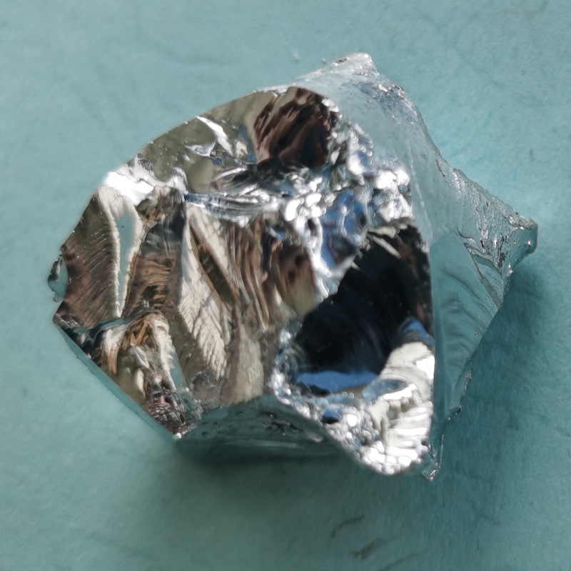
Bismuth Selenide
Bismuth Selenide Bi2Se3, black crystal appearance, CAS 12068-69-8, MW 654.84, melting point 710°C, boiling point 1007°C, density 6.82g/cm3, rhomb and hexagonal Structure, is insoluble in water and organic solvents. but soluble in strong acids, decomposes when heated in air, and decomposes in nitric acid and aqua regia. Bismuth selenide Bi2Se3 belongs to group 15 (VA) post-transition metal trichalcogenides, which is predicted to be 3D strong topological insulator with topologically non-trivial energy gap of 0.3 eV. Bismuth Selenide crystal is an indirect band gap semiconductor synthesized by hydrothermal method, Bridgeman R, direct method and zone floating method etc, the synthesized material is utilized to deposit bismuth selenide thin film at various substrate temperatures. Polycrystalline stoichiometric Bi2Se3 thin film is of N-type and carrier concentration of 1.02×1019 cm-3 at room temperature. Bismuth selenide powder is suitable for liquid chemical exfoliation to prepare Bi2Se3 nanosheets and nanoparticles. Bulk single Bismuth Selenide crystal is most commonly used as source from which single or few-layer sheets can be obtained by mechanical or liquid exfoliation. With remarkable thermoelectric and photoelectric properties, Bismuth selenide finds application in advanced photodetectors, magnetic devices, FETs, lasers, sputtering target, gas sensors, thermoelectric material, thin film solar cells, and quantum computing devices, Bismuth Selenide Bi2Se3 is also attractive to biomedicine due to the good bioactivity and biocompatibility. Bismuth Selenide Bi2Se3 at Western Minmetals (SC) Corporation with purity of 99.99% 4N, 99.995% 4N5, 99.999% 5N can be delivered in form of powder, granule, lump, chunk, blank, bulk crystal and single crystal etc or as customized specification.
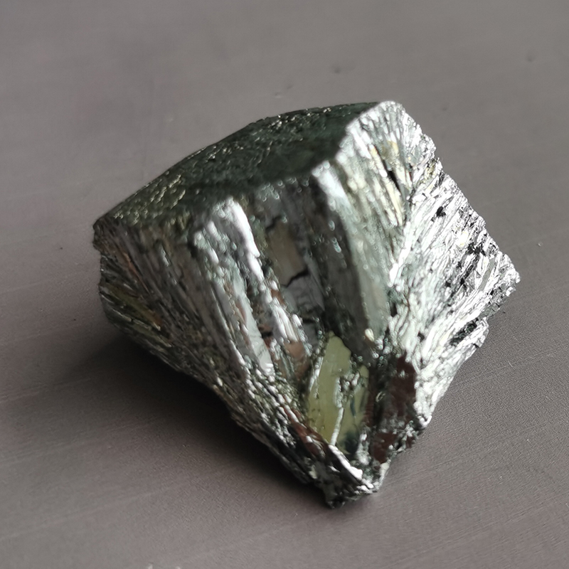
Gallium Selenide
Gallium Selenide or Gallium Triselenide Ga2Se3, CAS 12024-11-2, molecular mass148.68, melting point 960°C density 5.030g/cm3, a dark brown, shiny flake crystal with hexagonal structure, is a compound of Gallium and Selenium by chemical vapor deposition CVD method. GaSe is a layered semiconductor belongs to the family of metal chalcogens that crystallize in a layered structure. With the decrease of temperature, the maximum value of photoelectric effect of GaSe moves to the direction of short wave. Gallium Selenide GaSe crystal can be synthesized through different growth techniques of Bridgman growth, chemical vapor transport CVT and flux zone growth to optimize grain sizes and reduce defect concentrations. Gallium selenide GaSe crystal is proposed as the active compound for use in photovoltaic devices suited towards electronic and optical applications in 2D materials field, as intercalation electrodes in electrochemical lithium cells, and as a nonlinear optical medium. Gallium Selenide Ga2Se3 at Western Minmetals (SC) Corporation with purity of 99.99% 4N, 99.999% 5N can be delivered in form of powder, granule, lump, chunk, blank, bulk crystal and single crystal etc or as customized specification.
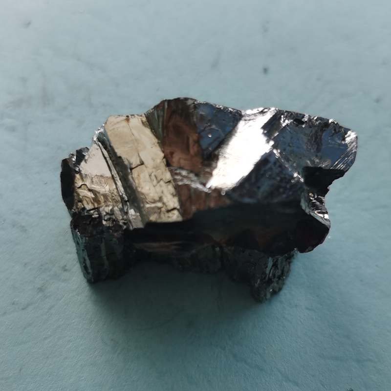
Indium Selenide

Indium Selenide, or Diinsium Triselenide In2Se3, black to dull grease luster powder or lump, CAS No 2056-07-4, melting point 660°C, density 5.55g/cm3, is a compound of indium and selenium, which is stable under room temperature and pressure, and kept to avoid light, open fire and high temperature. It is soluble in strong acid and easy to decompose. The semiconductive compound In2Se3 has a defective ZnS lattice structure in which the non-metallic atoms are arranged in tetrahedron by three metal atoms and one vacancy. To ensure structural, optical, and electronic consistency, Indium Selenide or Diindium Triselenide InSe is developed by Brigmann method preferable to offer highly crystallization as well as large size. Besides, the Flux Zone Growth and Chemical Vapor Transport CVT growth techniques are also optional. In2Se3 crystal is a direct gap semiconductor of 1.56eV emission (300K), α- In2Se3 and β- In2Se3 crystals are the two most common forms with defect wurtzite structures. It is mainly used as semiconductor, optical materials, photovoltaic devices, electrical sensors, or to be used for preparing copper indium gallium selenium CIGS thin film material. Indium Selenide InSe at Western Minmetals (SC) Corporation with 99.99% 4N, 99.999% 5N purity can be delivered in form of powder, granule, lump, chunk, blank, bulk crystal etc or as customized specification.
- Sample Available Upon Request
- Safety Delivery of Goods By Courier/Air/Sea
- COA/COC Quality Management
- Secure & Convenient Packing
- UN Standard Packing Available Upon Request
- ISO9001:2015 Certified
- CPT/CIP/FOB/CFR Terms By Incoterms 2010
- Flexible Payment Terms T/T D/P L/C Acceptable
- Full Dimensional After-Sale Services
- Quality Inspection By Sate-of-the-art Facility
- Rohs/REACH Regulations Approval
- Non-Disclosure Agreements NDA
- Non-Conflict Mineral Policy
- Regular Environmental Management Review
- Social Responsibility Fulfillment


- English
- French
- German
- Portuguese
- Spanish
- Russian
- Japanese
- Korean
- Arabic
- Irish
- Greek
- Turkish
- Italian
- Danish
- Romanian
- Indonesian
- Czech
- Afrikaans
- Swedish
- Polish
- Basque
- Catalan
- Esperanto
- Hindi
- Lao
- Albanian
- Amharic
- Armenian
- Azerbaijani
- Belarusian
- Bengali
- Bosnian
- Bulgarian
- Cebuano
- Chichewa
- Corsican
- Croatian
- Dutch
- Estonian
- Filipino
- Finnish
- Frisian
- Galician
- Georgian
- Gujarati
- Haitian
- Hausa
- Hawaiian
- Hebrew
- Hmong
- Hungarian
- Icelandic
- Igbo
- Javanese
- Kannada
- Kazakh
- Khmer
- Kurdish
- Kyrgyz
- Latin
- Latvian
- Lithuanian
- Luxembou..
- Macedonian
- Malagasy
- Malay
- Malayalam
- Maltese
- Maori
- Marathi
- Mongolian
- Burmese
- Nepali
- Norwegian
- Pashto
- Persian
- Punjabi
- Serbian
- Sesotho
- Sinhala
- Slovak
- Slovenian
- Somali
- Samoan
- Scots Gaelic
- Shona
- Sindhi
- Sundanese
- Swahili
- Tajik
- Tamil
- Telugu
- Thai
- Ukrainian
- Urdu
- Uzbek
- Vietnamese
- Welsh
- Xhosa
- Yiddish
- Yoruba
- Zulu