
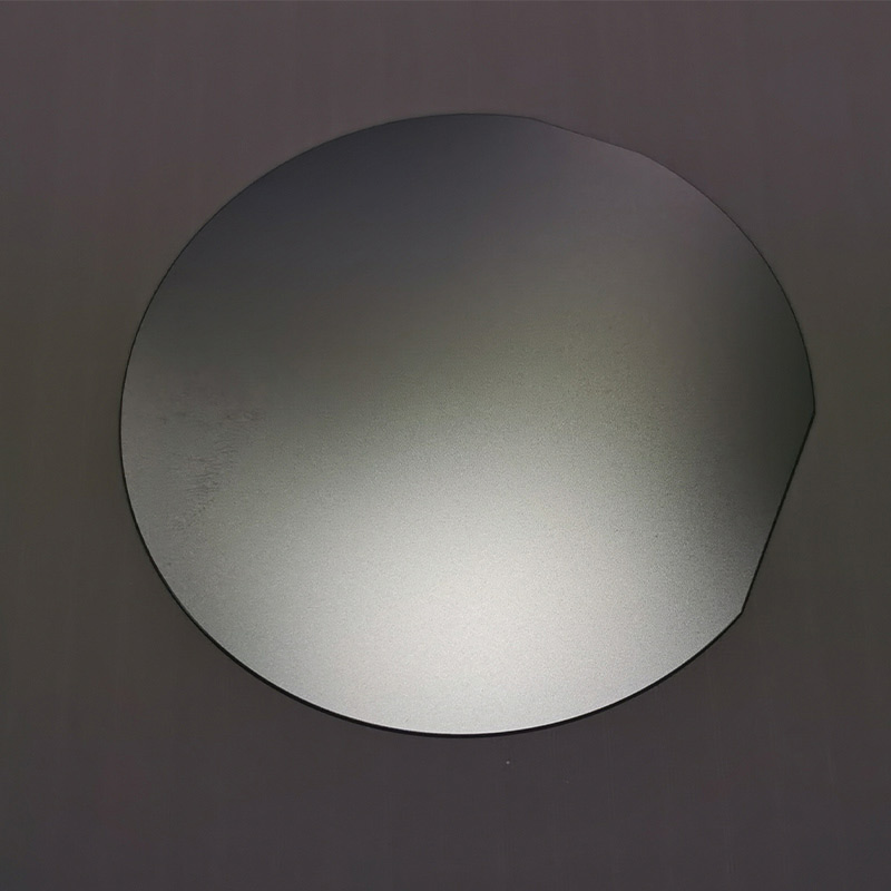


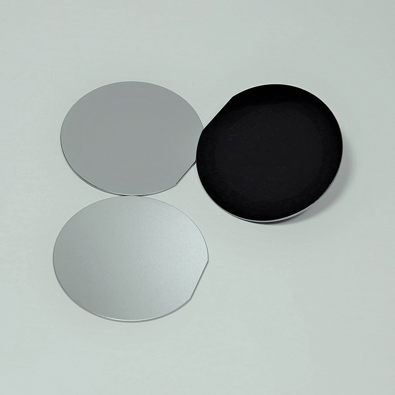
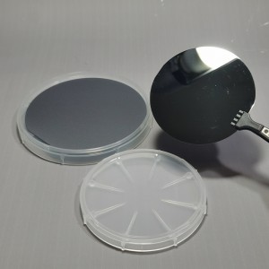
FZ NTD Silicon Wafer
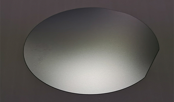
As a market leading supplier of FZ NTD silicon for promising power applications, and following the growing demands for top quality level wafers, superior FZ NTD silicon wafer at Western Minmetals (SC) Corporation can be offered to our customers worldwide in various size ranging from 2″ to 6″ in diameter (50, 75, 100, 125 and 150mm) and wide range of resistivity 5 to 2000 ohm-cm in <1-1-1>, <1-1-0>, <1-0-0> orientations with lapped, etched and polished surface finish in package of foam box or cassette, carton box outside or as customized specification to the perfect solution.
| No. | Items | Standard Specification | ||||
| 1 | Size | 2" | 3" | 4" | 5" | 6" |
| 2 | Diameter | 50.8±0.3 | 76.2±0.3 | 100±0.5 | 125±0.5 | 150±0.5 |
| 3 | Conductivity | n-type | n-type | n-type | n-type | n-type |
| 4 | Orientation | <100>, <111>, <110> | ||||
| 5 | Thickness μm | 279, 381, 425, 525, 575, 625, 675, 725 or as required | ||||
| 6 | Resistivity Ω-cm | 36-44, 44-52, 90-110, 100-250, 200-400 or as required | ||||
| 7 | RRV max | 8%, 10%, 12% | ||||
| 8 | TTV μm max | 10 | 10 | 10 | 10 | 10 |
| 9 | Bow/Warp μm max | 30 | 30 | 30 | 30 | 30 |
| 10 | Carrier Lifetime μs | >200, >300, >400 or as required | ||||
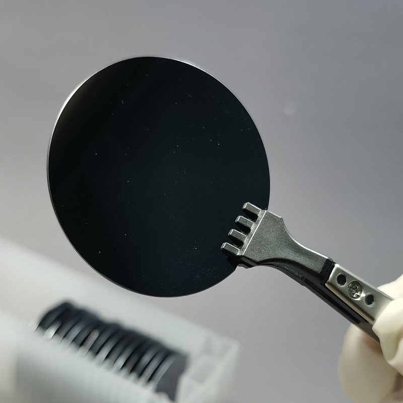
| 11 | Surface Finish | As-cut,Lapped,Polished | ||||
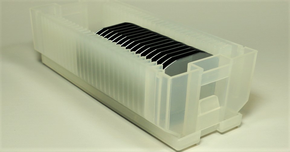
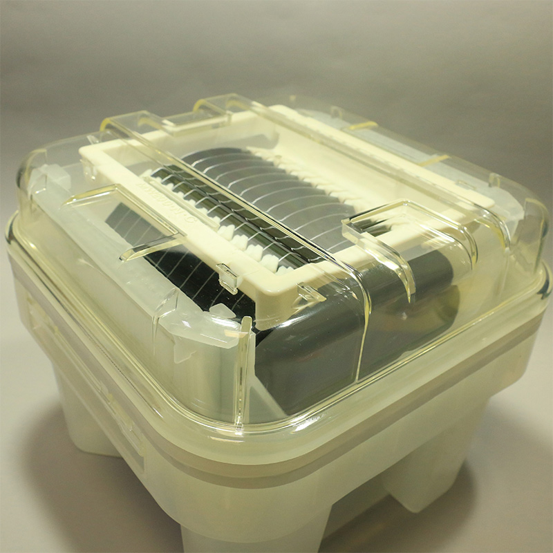
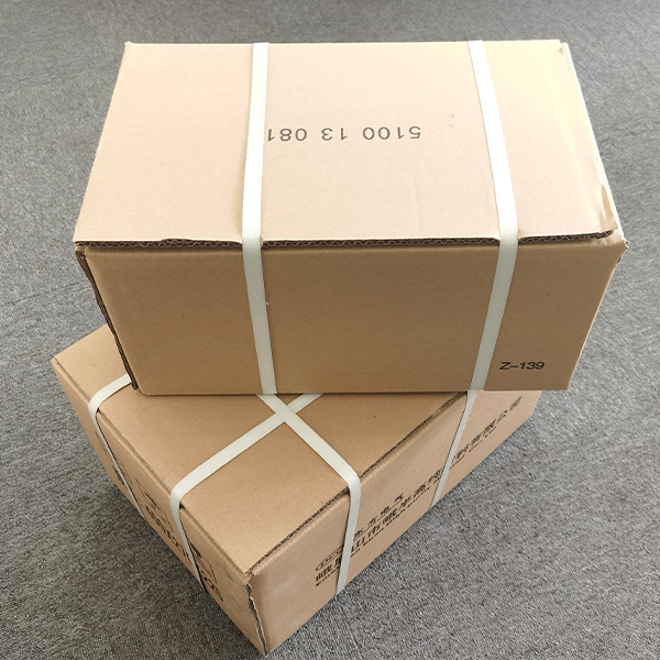
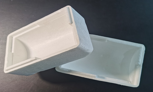
| 12 | Packing | Foam box inside, carton box outside. | ||||
| Symbol | Si |
| Atomic Number | 14 |
| Atomic Weight | 28.09 |
| Element Category | Metalloid |
| Group, Period, Block | 14, 3, P |
| Crystal structure | Diamond |
| Color | Dark gray |
| Melting Point | 1414°C, 1687.15 K |
| Boiling Point | 3265°C, 3538.15 K |
| Density at 300K | 2.329 g/cm3 |
| Intrinsic resistivity | 3.2E5 Ω-cm |
| CAS Number | 7440-21-3 |
| EC Number | 231-130-8 |
FZ-NTD Silicon Wafer is a paramount importance for applications in high power, detector technologies and in semiconductor devices that have to work in extreme conditions or where low resistivity variation across the wafer is required, such as gate-turn-off thyristor GTO, static induction thyristor SITH, giant transistor GTR, insulate-gate bipolar transistor IGBT, extra HV diode PIN. FZ NTD n-type silicon wafer is also as main functional material for various frequency converters, rectifiers, large-power control elements, new power electronic devices, photoelectronic devices, silicon rectifier SR, silicon control SCR, and optical components such as lenses and windows for terahertz applications.
- Sample Available Upon Request
- Safety Delivery of Goods By Courier/Air/Sea
- COA/COC Quality Management
- Secure & Convenient Packing
- UN Standard Packing Available Upon Request
- ISO9001:2015 Certified
- CPT/CIP/FOB/CFR Terms By Incoterms 2010
- Flexible Payment Terms T/T D/P L/C Acceptable
- Full Dimensional After-Sale Services
- Quality Inspection By Sate-of-the-art Facility
- Rohs/REACH Regulations Approval
- Non-Disclosure Agreements NDA
- Non-Conflict Mineral Policy
- Regular Environmental Management Review
- Social Responsibility Fulfillment


- English
- French
- German
- Portuguese
- Spanish
- Russian
- Japanese
- Korean
- Arabic
- Irish
- Greek
- Turkish
- Italian
- Danish
- Romanian
- Indonesian
- Czech
- Afrikaans
- Swedish
- Polish
- Basque
- Catalan
- Esperanto
- Hindi
- Lao
- Albanian
- Amharic
- Armenian
- Azerbaijani
- Belarusian
- Bengali
- Bosnian
- Bulgarian
- Cebuano
- Chichewa
- Corsican
- Croatian
- Dutch
- Estonian
- Filipino
- Finnish
- Frisian
- Galician
- Georgian
- Gujarati
- Haitian
- Hausa
- Hawaiian
- Hebrew
- Hmong
- Hungarian
- Icelandic
- Igbo
- Javanese
- Kannada
- Kazakh
- Khmer
- Kurdish
- Kyrgyz
- Latin
- Latvian
- Lithuanian
- Luxembou..
- Macedonian
- Malagasy
- Malay
- Malayalam
- Maltese
- Maori
- Marathi
- Mongolian
- Burmese
- Nepali
- Norwegian
- Pashto
- Persian
- Punjabi
- Serbian
- Sesotho
- Sinhala
- Slovak
- Slovenian
- Somali
- Samoan
- Scots Gaelic
- Shona
- Sindhi
- Sundanese
- Swahili
- Tajik
- Tamil
- Telugu
- Thai
- Ukrainian
- Urdu
- Uzbek
- Vietnamese
- Welsh
- Xhosa
- Yiddish
- Yoruba
- Zulu