

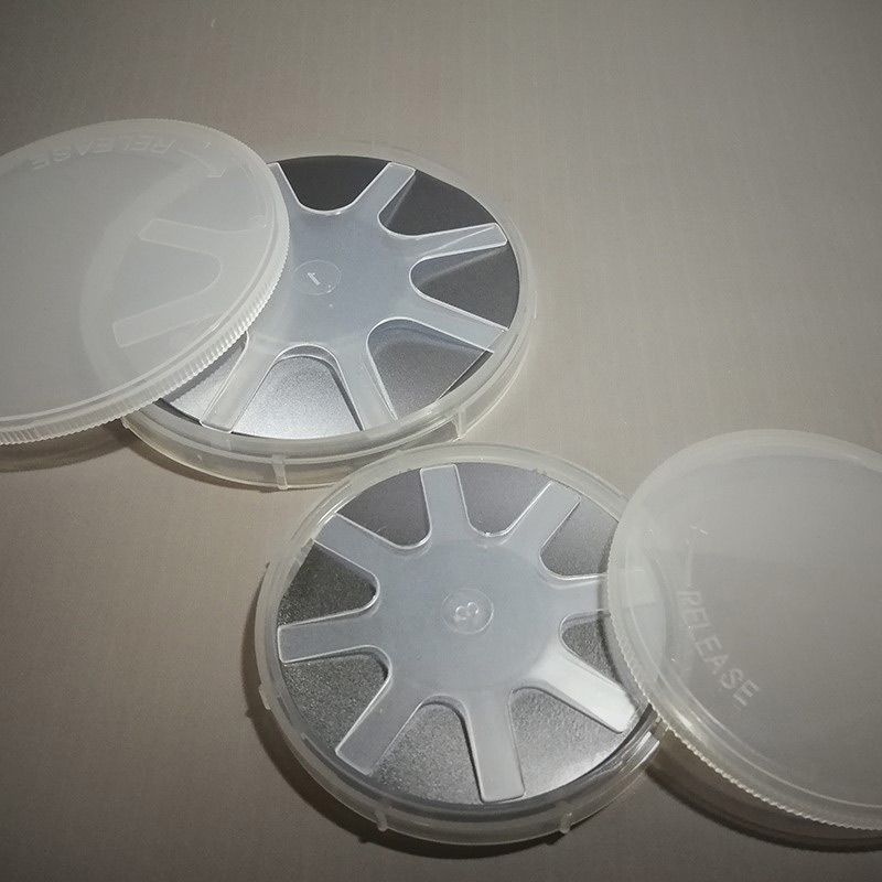
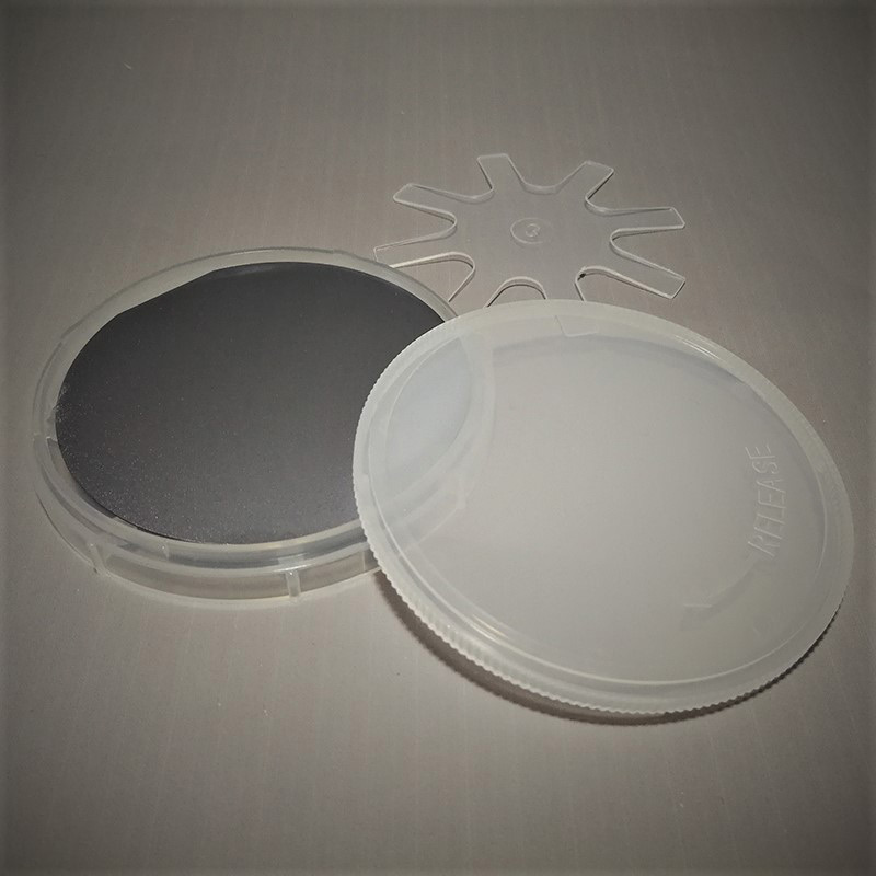
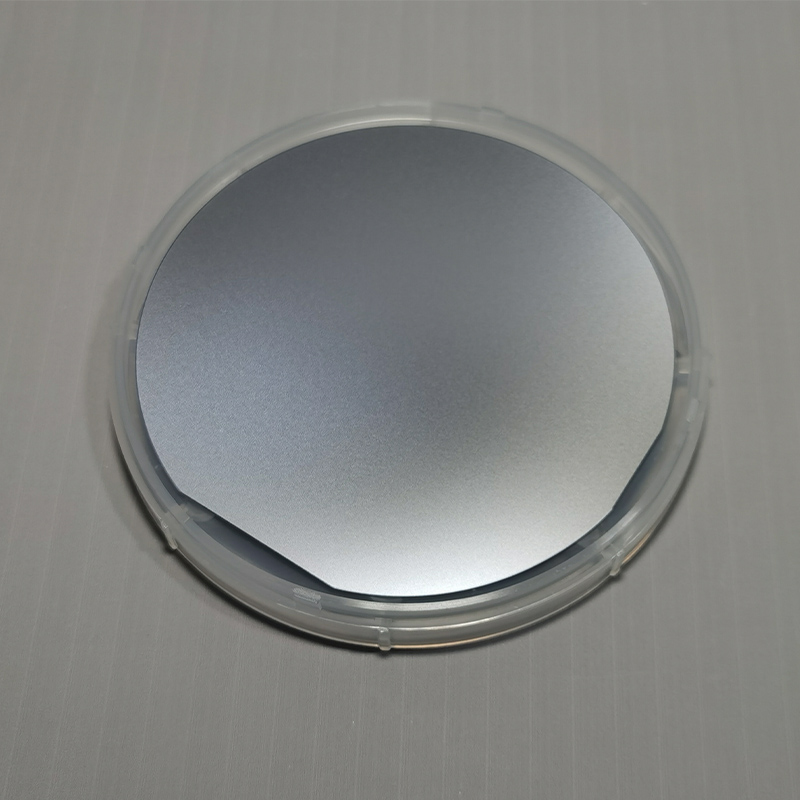
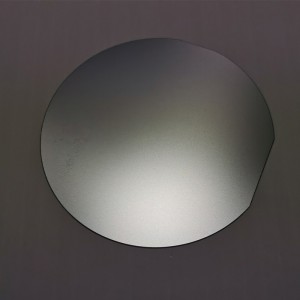
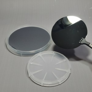
Epi Silicon Wafer
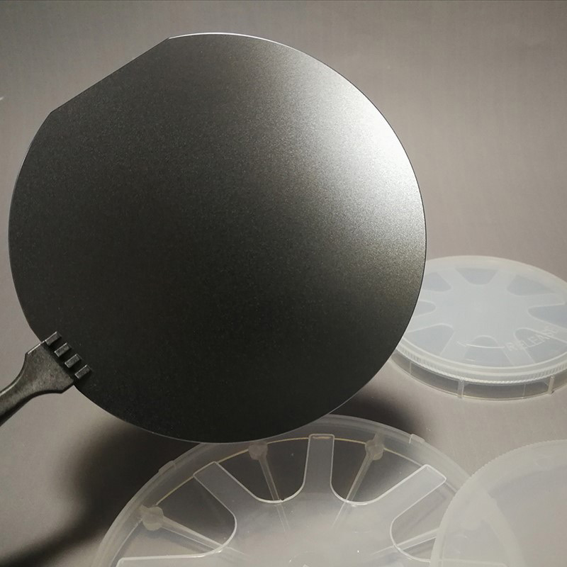
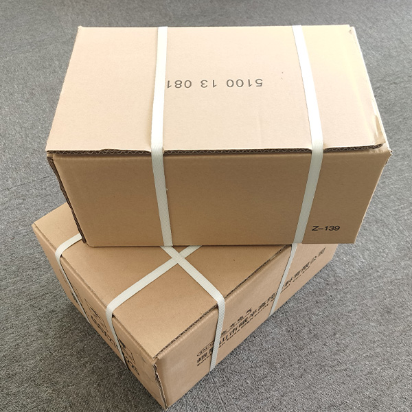
Epitaxial Silicon Wafers or EPI Silicon Wafer at Western Minmetals (SC) Corporation can be offered in size of 4, 5 and 6 inch (100mm, 125mm, 150mm diameter), with orientation <100>, <111>, epilayer resistivity of <1ohm-cm or up to 150ohm-cm, and epilayer thickness of<1um or up to 150um, to satisfy the various requirements in surface finish of etched or LTO treatment, packed in cassette with carton box outside, or as customized specification to the perfect solution.
| Symbol | Si |
| Atomic Number | 14 |
| Atomic Weight | 28.09 |
| Element Category | Metalloid |
| Group, Period, Block | 14, 3, P |
| Crystal structure | Diamond |
| Color | Dark gray |
| Melting Point | 1414°C, 1687.15 K |
| Boiling Point | 3265°C, 3538.15 K |
| Density at 300K | 2.329 g/cm3 |
| Intrinsic resistivity | 3.2E5 Ω-cm |
| CAS Number | 7440-21-3 |
| EC Number | 231-130-8 |
| No. | Items | Standard Specification | ||
| 1 | General Characteristics | |||
| 1-1 | Size | 4" | 5" | 6" |
| 1-2 | Diameter mm | 100±0.5 | 125±0.5 | 150±0.5 |
| 1-3 | Orientation | <100>, <111> | <100>, <111> | <100>, <111> |
| 2 | Epitaxial Layer Characteristics | |||
| 2-1 | Growth Method | CVD | CVD | CVD |
| 2-2 | Conductivity Type | P or P+, N/ or N+ | P or P+, N/ or N+ | P or P+, N/ or N+ |
| 2-3 | Thickness μm | 2.5-120 | 2.5-120 | 2.5-120 |
| 2-4 | Thickness Uniformity | ≤3% | ≤3% | ≤3% |
| 2-5 | Resistivity Ω-cm | 0.1-50 | 0.1-50 | 0.1-50 |
| 2-6 | Resistivity Uniformity | ≤3% | ≤5% | - |
| 2-7 | Dislocation cm-2 | <10 | <10 | <10 |
| 2-8 | Surface Quality | No chip, haze or orange peel remains, etc. | ||
| 3 | Handle Substrate Characteristics | |||
| 3-1 | Growth Method | CZ | CZ | CZ |
| 3-2 | Conductivity Type | P/N | P/N | P/N |
| 3-3 | Thickness μm | 525-675 | 525-675 | 525-675 |
| 3-4 | Thickness Uniformity max | 3% | 3% | 3% |
| 3-5 | Resistivity Ω-cm | As required | As required | As required |
| 3-6 | Resistivity Uniformity | 5% | 5% | 5% |
| 3-7 | TTV μm max | 10 | 10 | 10 |
| 3-8 | Bow μm max | 30 | 30 | 30 |
| 3-9 | Warp μm max | 30 | 30 | 30 |
| 3-10 | EPD cm-2 max | 100 | 100 | 100 |
| 3-11 | Edge Profile | Rounded | Rounded | Rounded |
| 3-12 | Surface Quality | No chip, haze or orange peel remains, etc. | ||
| 3-13 | Back Side Finish | Etched or LTO (5000±500Å) | ||
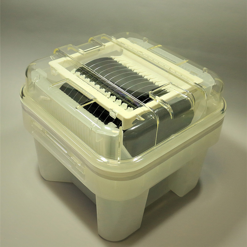
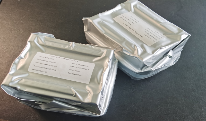
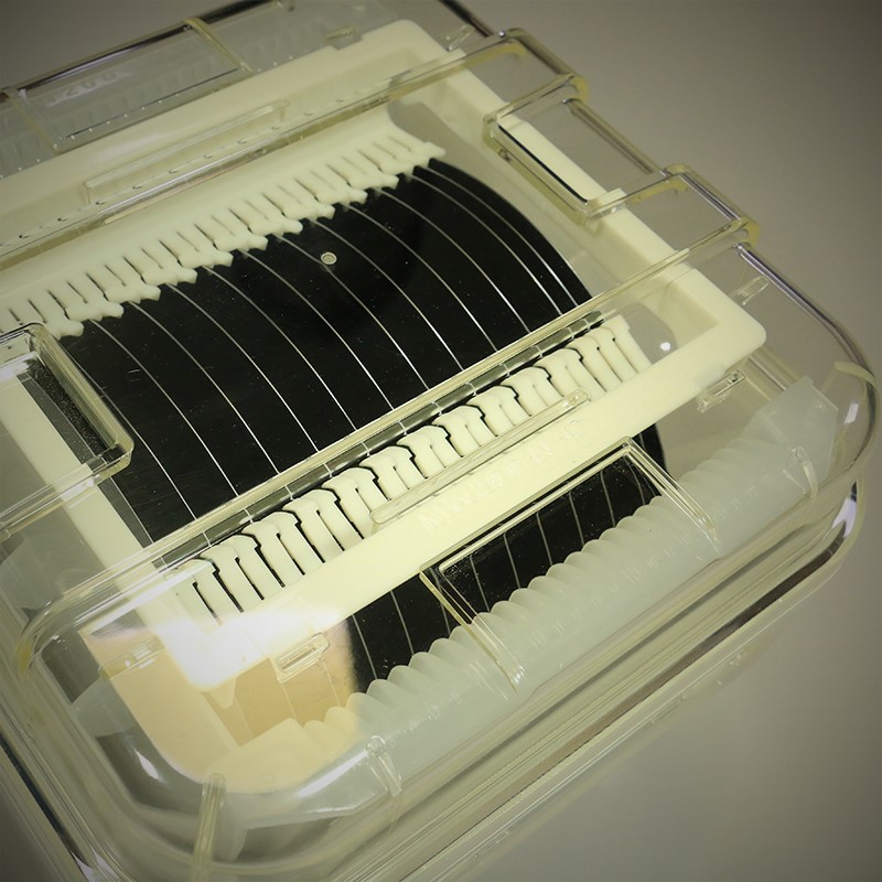
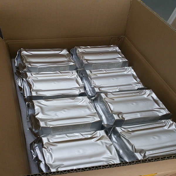
| 4 | Packing | Cassette inside, carton box outside. | ||
Silicon Epitaxial Wafers are primarily used in the production of advanced semiconductor devices, highly integrated semiconductor elements ICs, discrete and power devices, also utilized for element of diode and transistor or substrate for IC such as bipolar type, MOS and BiCMOS devices. Furthermore, multiple layer epitaxial and thick film EPI silicon wafers are often used in microelectronics, photonics and photovoltaics application.

- Sample Available Upon Request
- Safety Delivery of Goods By Courier/Air/Sea
- COA/COC Quality Management
- Secure & Convenient Packing
- UN Standard Packing Available Upon Request
- ISO9001:2015 Certified
- CPT/CIP/FOB/CFR Terms By Incoterms 2010
- Flexible Payment Terms T/T D/P L/C Acceptable
- Full Dimensional After-Sale Services
- Quality Inspection By Sate-of-the-art Facility
- Rohs/REACH Regulations Approval
- Non-Disclosure Agreements NDA
- Non-Conflict Mineral Policy
- Regular Environmental Management Review
- Social Responsibility Fulfillment


- English
- French
- German
- Portuguese
- Spanish
- Russian
- Japanese
- Korean
- Arabic
- Irish
- Greek
- Turkish
- Italian
- Danish
- Romanian
- Indonesian
- Czech
- Afrikaans
- Swedish
- Polish
- Basque
- Catalan
- Esperanto
- Hindi
- Lao
- Albanian
- Amharic
- Armenian
- Azerbaijani
- Belarusian
- Bengali
- Bosnian
- Bulgarian
- Cebuano
- Chichewa
- Corsican
- Croatian
- Dutch
- Estonian
- Filipino
- Finnish
- Frisian
- Galician
- Georgian
- Gujarati
- Haitian
- Hausa
- Hawaiian
- Hebrew
- Hmong
- Hungarian
- Icelandic
- Igbo
- Javanese
- Kannada
- Kazakh
- Khmer
- Kurdish
- Kyrgyz
- Latin
- Latvian
- Lithuanian
- Luxembou..
- Macedonian
- Malagasy
- Malay
- Malayalam
- Maltese
- Maori
- Marathi
- Mongolian
- Burmese
- Nepali
- Norwegian
- Pashto
- Persian
- Punjabi
- Serbian
- Sesotho
- Sinhala
- Slovak
- Slovenian
- Somali
- Samoan
- Scots Gaelic
- Shona
- Sindhi
- Sundanese
- Swahili
- Tajik
- Tamil
- Telugu
- Thai
- Ukrainian
- Urdu
- Uzbek
- Vietnamese
- Welsh
- Xhosa
- Yiddish
- Yoruba
- Zulu