


Indium Antimonide
InSb

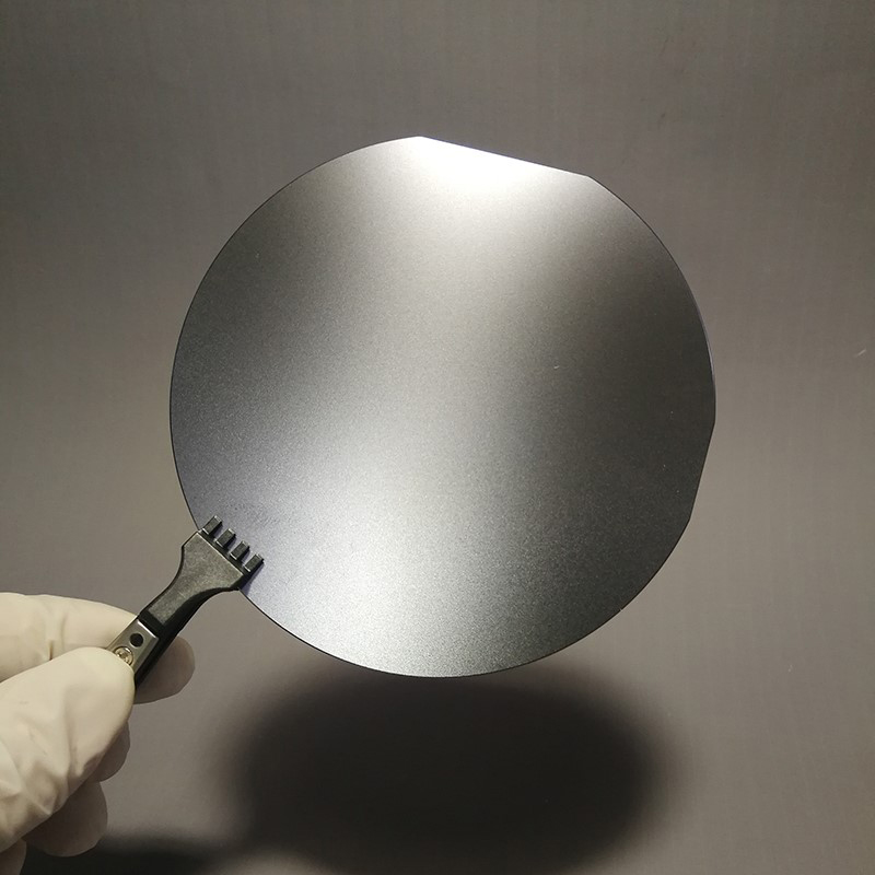
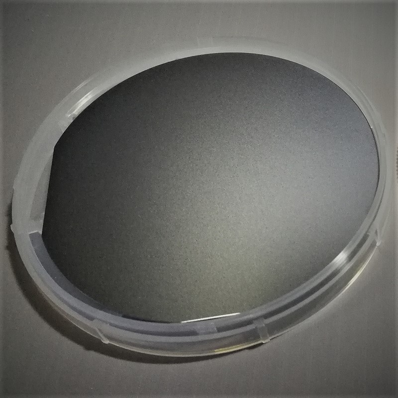
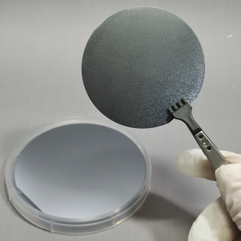
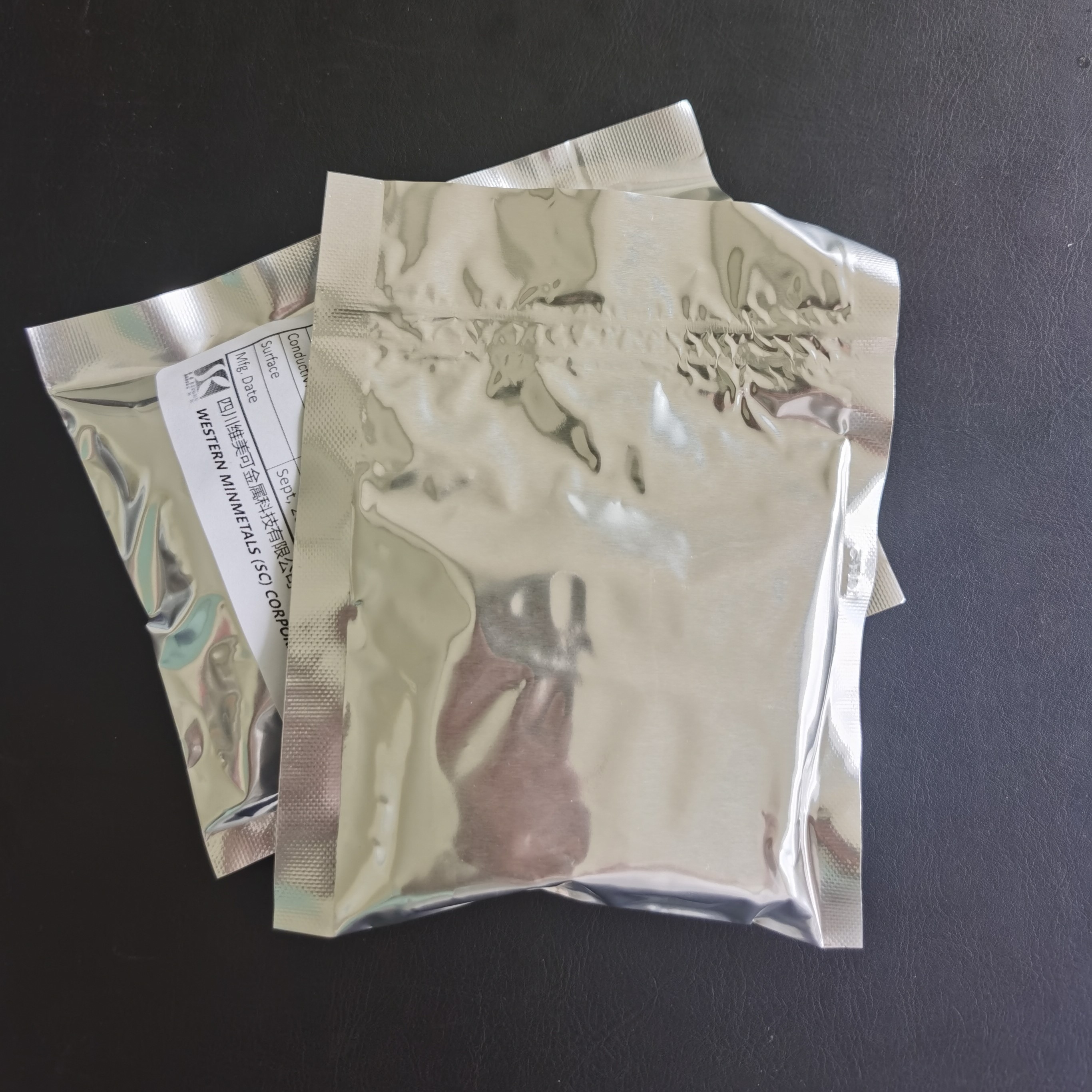
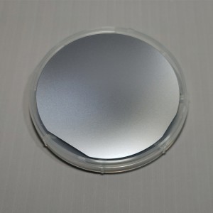
Indium Antimonide Substrate (InSb Substrate, InSb Wafer) n-type or p-type at Western Minmetals (SC) Corporation can be offered in size of 1" 2" 3" and 4” (30, 50, 75 and 100mm) diameter, orientation <111> or <100>, and with wafer surface of lapped, etched, polished finishes. Indium Antimonide Single Crystal bar (InSb Monocrystal bar) can also be supplied upon request.
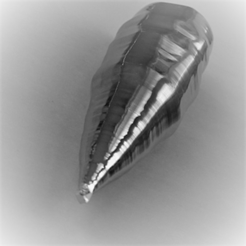
Indium Antimonide Polycrystalline (InSb Polycrystalline, or multicrystal InSb) with size of irregular lump, or blank (15-40)x(40-80)mm are also customized upon request to the perfect solution.
Meanwhile, Indium Antimonide Target (InSb Target) of Dia.50-80mm with un-doped n-type is also available.
| No. | Items | Standard Specification | ||
| 1 | Indium Antimonide Substrate | 2" | 3" | 4" |
| 2 | Diameter mm | 50.5±0.5 | 76.2±0.5 | 100±0.5 |
| 3 | Growth Method | LEC | LEC | LEC |
| 4 | Conductivity | P-type/Zn,Ge doped, N-type/Te-doped, Un-doped | ||
| 5 | Orientation | (100)±0.5°, (111)±0.5° | ||
| 6 | Thickness μm | 500±25 | 600±25 | 800±25 |
| 7 | Orientation Flat mm | 16±2 | 22±1 | 32.5±1 |
| 8 | Identification Flat mm | 8±1 | 11±1 | 18±1 |
| 9 | Mobility cm2/V.s | 1-7E5 N/un-doped, 3E5-2E4 N/Te-doped, 8-0.6E3 or ≤8E13 P/Ge-doped | ||
| 10 | Carrier Concentration cm-3 | 6E13-3E14 N/un-doped, 3E14-2E18 N/Te-doped, 1E14-9E17 or <1E14 P/Ge-doped | ||
| 11 | TTV μm max | 15 | 15 | 15 |
| 12 | Bow μm max | 15 | 15 | 15 |
| 13 | Warp μm max | 20 | 20 | 20 |
| 14 | Dislocation Density cm-2 max | 50 | 50 | 50 |
| 15 | Surface Finish | P/E, P/P | P/E, P/P | P/E, P/P |
| 16 | Packing | Single wafer container sealed in Aluminum bag. | ||
|
No. |
Items |
Standard Specification |
|
|
Indium Antimonide Polycrystalline |
Indium Antimonide Target |
||
|
1 |
Conductivity |
Undoped |
Undoped |
|
2 |
Carrier Concentration cm-3 |
6E13-3E14 |
1.9-2.1E16 |
|
3 |
Mobility cm2/V.s |
5-7E5 |
6.9-7.9E4 |
|
4 |
Size |
15-40x40-80 mm |
D(50-80) mm |
|
5 |
Packing |
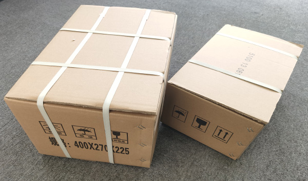
In composite aluminum bag, carton box outside |
|
| Linear Formula | InSb |
| Molecular Weight | 236.58 |
| Crystal structure | Zinc blende |
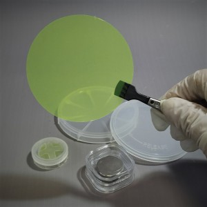
| Appearance | Dark grey metallic crystals |
| Melting Point | 527 °C |
| Boiling Point | N/A |
| Density at 300K | 5.78 g/cm3 |
| Energy Gap | 0.17 eV |
| Intrinsic resistivity | 4E(-3) Ω-cm |
| CAS Number | 1312-41-0 |
| EC Number | 215-192-3 |
Indium Antimonide InSb wafer is one ideal substrate for the production of many state-of-art components and devices, such as advanced thermal imaging solution, FLIR system, hall element and magnetoresistance effect element, infrared homing missile guidance system, highly-responsive Infrared photodetector sensor, high-precision magnetic and rotary resistivity sensor, focal planar arrays, and also adapted as a terahertz radiation source and in infrared astronomical space telescope etc.
- Sample Available Upon Request
- Safety Delivery of Goods By Courier/Air/Sea
- COA/COC Quality Management
- Secure & Convenient Packing
- UN Standard Packing Available Upon Request
- ISO9001:2015 Certified
- CPT/CIP/FOB/CFR Terms By Incoterms 2010
- Flexible Payment Terms T/T D/P L/C Acceptable
- Full Dimensional After-Sale Services
- Quality Inspection By Sate-of-the-art Facility
- Rohs/REACH Regulations Approval
- Non-Disclosure Agreements NDA
- Non-Conflict Mineral Policy
- Regular Environmental Management Review
- Social Responsibility Fulfillment


- English
- French
- German
- Portuguese
- Spanish
- Russian
- Japanese
- Korean
- Arabic
- Irish
- Greek
- Turkish
- Italian
- Danish
- Romanian
- Indonesian
- Czech
- Afrikaans
- Swedish
- Polish
- Basque
- Catalan
- Esperanto
- Hindi
- Lao
- Albanian
- Amharic
- Armenian
- Azerbaijani
- Belarusian
- Bengali
- Bosnian
- Bulgarian
- Cebuano
- Chichewa
- Corsican
- Croatian
- Dutch
- Estonian
- Filipino
- Finnish
- Frisian
- Galician
- Georgian
- Gujarati
- Haitian
- Hausa
- Hawaiian
- Hebrew
- Hmong
- Hungarian
- Icelandic
- Igbo
- Javanese
- Kannada
- Kazakh
- Khmer
- Kurdish
- Kyrgyz
- Latin
- Latvian
- Lithuanian
- Luxembou..
- Macedonian
- Malagasy
- Malay
- Malayalam
- Maltese
- Maori
- Marathi
- Mongolian
- Burmese
- Nepali
- Norwegian
- Pashto
- Persian
- Punjabi
- Serbian
- Sesotho
- Sinhala
- Slovak
- Slovenian
- Somali
- Samoan
- Scots Gaelic
- Shona
- Sindhi
- Sundanese
- Swahili
- Tajik
- Tamil
- Telugu
- Thai
- Ukrainian
- Urdu
- Uzbek
- Vietnamese
- Welsh
- Xhosa
- Yiddish
- Yoruba
- Zulu