


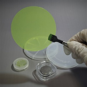
Gallium Nitride GaN

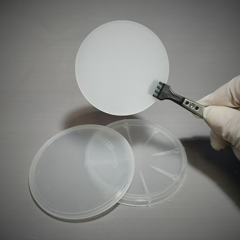
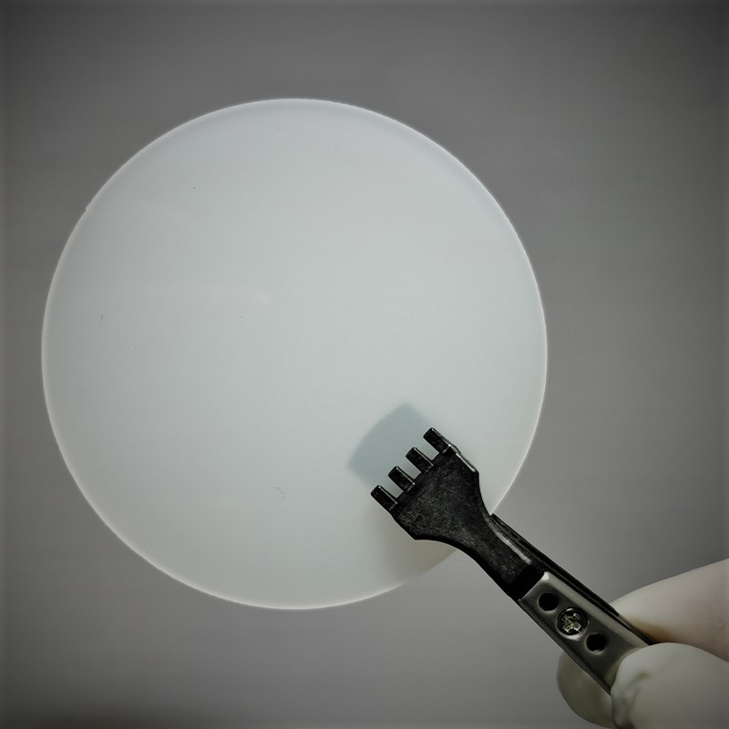
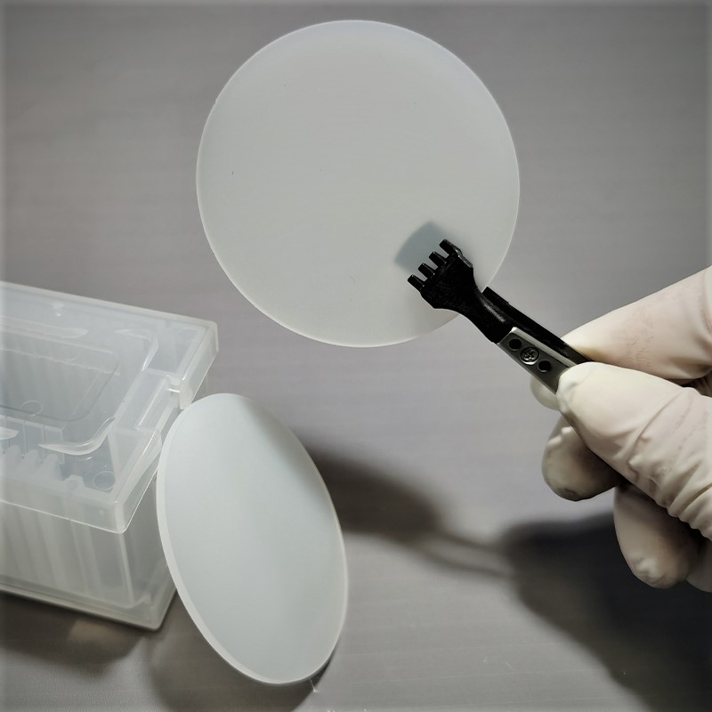
Gallium Nitride GaN at Western Minmetals (SC) Corporation can be provided in size of circular wafer 2 inch ” or 4 ” (50mm, 100mm) and square wafer 10×10 or 10×5 mm. Any customized size and specification are for the perfect solution to our customers worldwide.
| No. | Items | Standard Specification | ||
| 1 | Shape | Circular | Circular | Square |
| 2 | Size | 2" | 4" | -- |
| 3 | Diameter mm | 50.8±0.5 | 100±0.5 | -- |
| 4 | Side Length mm | -- | -- | 10x10 or 10x5 |
| 5 | Growth Method | HVPE | HVPE | HVPE |
| 6 | Orientation | C-plane (0001) | C-plane (0001) | C-plane (0001) |
| 7 | Conductivity Type | N-type/Si-doped, Un-doped, Semi-insulating | ||
| 8 | Resistivity Ω-cm | <0.1, <0.05, >1E6 | ||
| 9 | Thickness μm | 350±25 | 350±25 | 350±25 |
| 10 | TTV μm max | 15 | 15 | 15 |
| 11 | Bow μm max | 20 | 20 | 20 |
| 12 | EPD cm-2 | <5E8 | <5E8 | <5E8 |
| 13 | Surface Finish | P/E, P/P | P/E, P/P | P/E, P/P |
| 14 | Surface Roughness | Front: ≤0.2nm, Back: 0.5-1.5μm or ≤0.2nm | ||
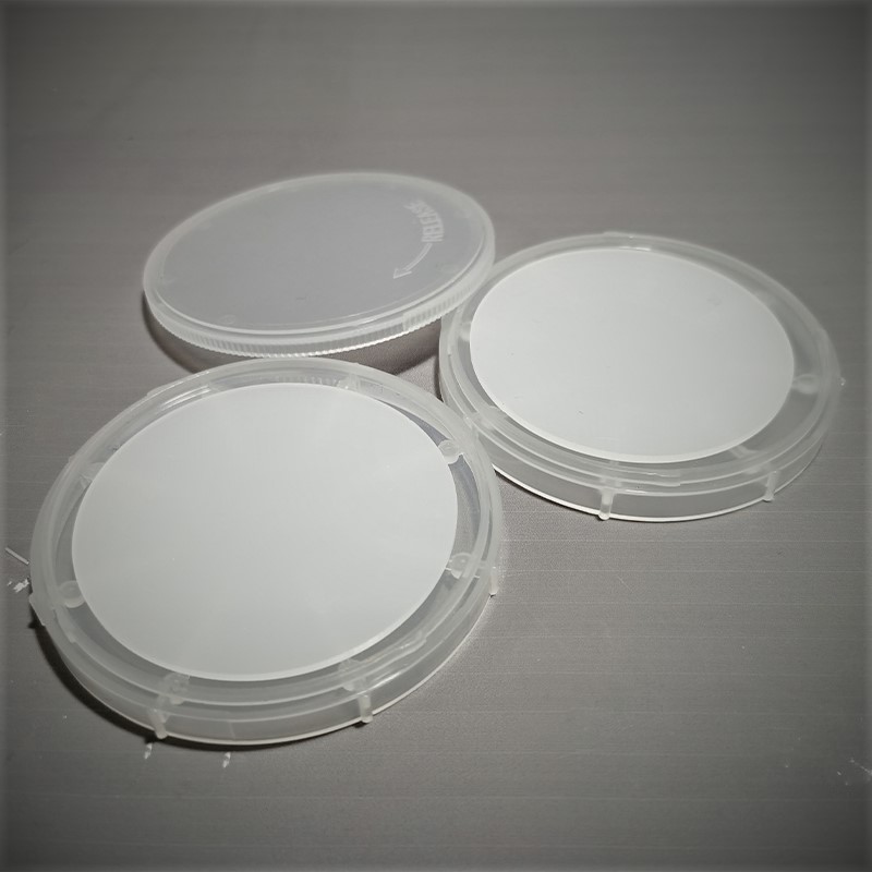
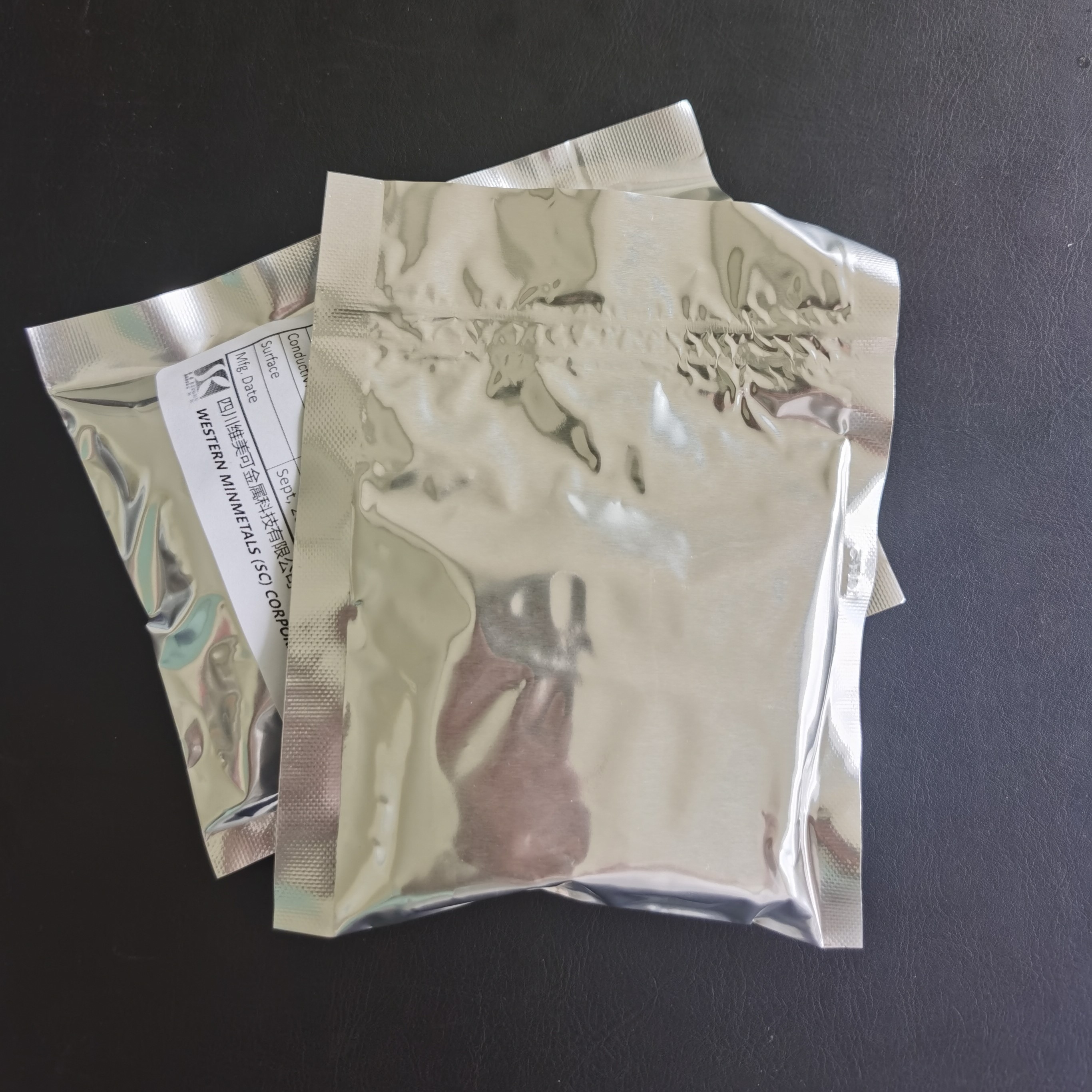
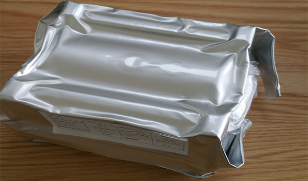
| 15 | Packing | Single wafer container sealed in Aluminum bag. | ||
| Linear Formula | GaN |
| Molecular Weight | 83.73 |
| Crystal structure | Zinc blende/Wurtzite |
| Appearance | Translucent solid |
| Melting Point | 2500 °C |
| Boiling Point | N/A |
| Density at 300K | 6.15 g/cm3 |
| Energy Gap | (3.2-3.29) eV at 300K |
| Intrinsic resistivity | >1E8 Ω-cm |
| CAS Number | 25617-97-4 |
| EC Number | 247-129-0 |
Gallium Nitride GaN is suitable for the production of the cutting-edge high speed and high capacity bright light-emitting diodes LEDs components, laser and optoelectronics devices such as green and blue lasers, high electron mobility transistors (HEMTs) products and in high-power and high-temperature devices manufacturing industry.
- Sample Available Upon Request
- Safety Delivery of Goods By Courier/Air/Sea
- COA/COC Quality Management
- Secure & Convenient Packing
- UN Standard Packing Available Upon Request
- ISO9001:2015 Certified
- CPT/CIP/FOB/CFR Terms By Incoterms 2010
- Flexible Payment Terms T/T D/P L/C Acceptable
- Full Dimensional After-Sale Services
- Quality Inspection By Sate-of-the-art Facility
- Rohs/REACH Regulations Approval
- Non-Disclosure Agreements NDA
- Non-Conflict Mineral Policy
- Regular Environmental Management Review
- Social Responsibility Fulfillment


- English
- French
- German
- Portuguese
- Spanish
- Russian
- Japanese
- Korean
- Arabic
- Irish
- Greek
- Turkish
- Italian
- Danish
- Romanian
- Indonesian
- Czech
- Afrikaans
- Swedish
- Polish
- Basque
- Catalan
- Esperanto
- Hindi
- Lao
- Albanian
- Amharic
- Armenian
- Azerbaijani
- Belarusian
- Bengali
- Bosnian
- Bulgarian
- Cebuano
- Chichewa
- Corsican
- Croatian
- Dutch
- Estonian
- Filipino
- Finnish
- Frisian
- Galician
- Georgian
- Gujarati
- Haitian
- Hausa
- Hawaiian
- Hebrew
- Hmong
- Hungarian
- Icelandic
- Igbo
- Javanese
- Kannada
- Kazakh
- Khmer
- Kurdish
- Kyrgyz
- Latin
- Latvian
- Lithuanian
- Luxembou..
- Macedonian
- Malagasy
- Malay
- Malayalam
- Maltese
- Maori
- Marathi
- Mongolian
- Burmese
- Nepali
- Norwegian
- Pashto
- Persian
- Punjabi
- Serbian
- Sesotho
- Sinhala
- Slovak
- Slovenian
- Somali
- Samoan
- Scots Gaelic
- Shona
- Sindhi
- Sundanese
- Swahili
- Tajik
- Tamil
- Telugu
- Thai
- Ukrainian
- Urdu
- Uzbek
- Vietnamese
- Welsh
- Xhosa
- Yiddish
- Yoruba
- Zulu