


Indium Arsenide
InAs
Indium Arsenide Crystal Wafer is a great substrate for making Hall devices and magnetic field sensor for its supreme hall mobility but narrow energy bandgap, an ideal material for the construction of infrared detectors with the wavelength range of 1–3.8 µm used in higher-power applications at room temperature, as well as mid wavelength infrared super lattice lasers, mid-infrared LEDs devices fabrication for its 2-14 μm wavelength range. Furthermore, InAs is an ideal substrate to further support the heterogeneous InGaAs, InAsSb, InAsPSb & InNAsSb or AlGaSb super lattice structure etc..
| No. | Items | Standard Specification | ||
| 1 | Size | 2" | 3" | 4" |
| 2 | Diameter mm | 50.5±0.5 | 76.2±0.5 | 100±0.5 |
| 3 | Growth Method | LEC | LEC | LEC |
| 4 | Conductivity | P-type/Zn-doped, N-type/S-doped, Un-doped | ||
| 5 | Orientation | (100)±0.5°, (111)±0.5° | ||
| 6 | Thickness μm | 500±25 | 600±25 | 800±25 |
| 7 | Orientation Flat mm | 16±2 | 22±2 | 32±2 |
| 8 | Identification Flat mm | 8±1 | 11±1 | 18±1 |
| 9 | Mobility cm2/V.s | 60-300, ≥2000 or as required | ||
| 10 | Carrier Concentration cm-3 | (3-80)E17 or ≤5E16 | ||
| 11 | TTV μm max | 10 | 10 | 10 |
| 12 | Bow μm max | 10 | 10 | 10 |
| 13 | Warp μm max | 15 | 15 | 15 |
| 14 | Dislocation Density cm-2 max | 1000 | 2000 | 5000 |
| 15 | Surface Finish | P/E, P/P | P/E, P/P | P/E, P/P |
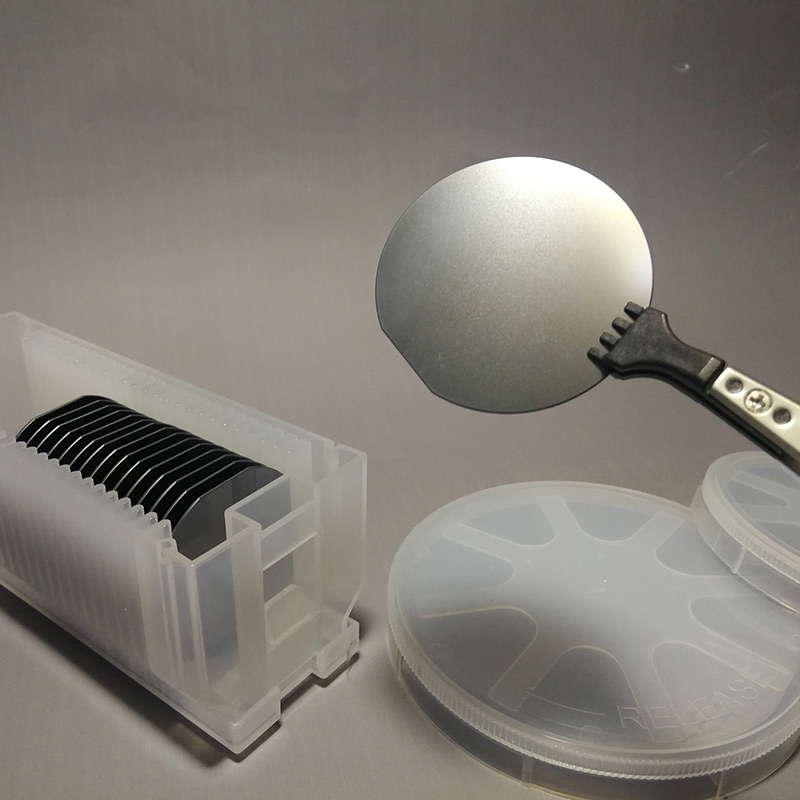
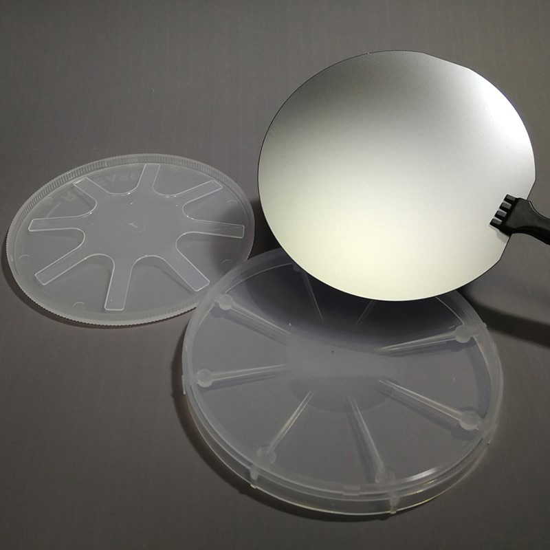
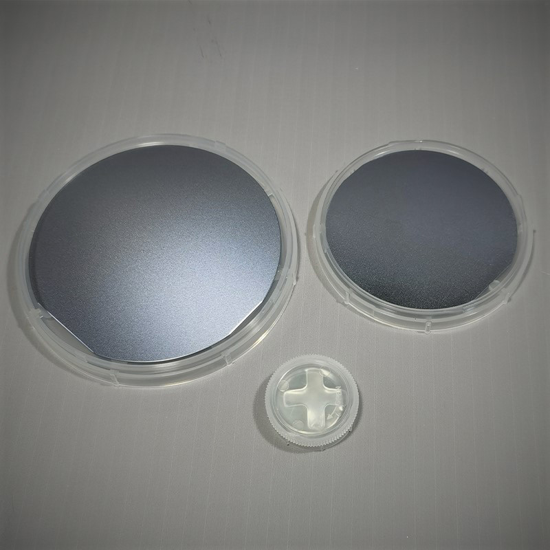
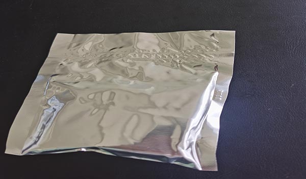
| 16 | Packing | Single wafer container sealed in Aluminum bag. | ||
| Linear Formula | InAs |
| Molecular Weight | 189.74 |
| Crystal structure | Zinc blende |
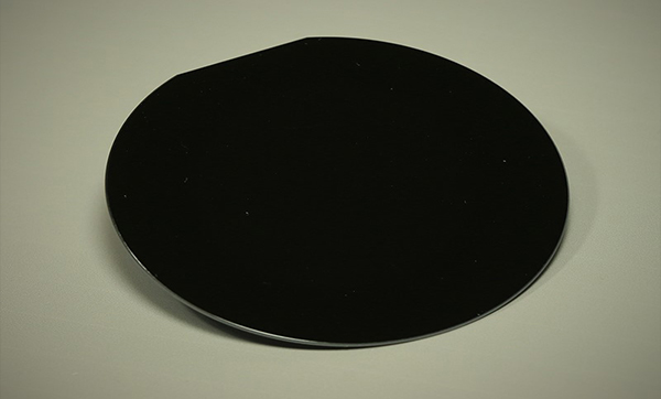
| Appearance | Gray crystalline solid |
| Melting Point | (936-942)°C |
| Boiling Point | N/A |
| Density at 300K | 5.67 g/cm3 |
| Energy Gap | 0.354 eV |
| Intrinsic Resistivity | 0.16 Ω-cm |
| CAS Number | 1303-11-3 |
| EC Number | 215-115-3 |
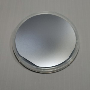
Indium Arsenide InAs at Western Minmetals (SC) Corporation can be supplied as polycrystalline lump or single crystal as-cut, etched, polished, or epi-ready wafers in a size of 2” 3”and 4” (50mm, 75mm,100mm) diameter, and p-type, n-type or un-doped conductivity and <111> or <100> orientation. The customized specification is for the perfect solution to our customers worldwide.
- Sample Available Upon Request
- Safety Delivery of Goods By Courier/Air/Sea
- COA/COC Quality Management
- Secure & Convenient Packing
- UN Standard Packing Available Upon Request
- ISO9001:2015 Certified
- CPT/CIP/FOB/CFR Terms By Incoterms 2010
- Flexible Payment Terms T/T D/P L/C Acceptable
- Full Dimensional After-Sale Services
- Quality Inspection By Sate-of-the-art Facility
- Rohs/REACH Regulations Approval
- Non-Disclosure Agreements NDA
- Non-Conflict Mineral Policy
- Regular Environmental Management Review
- Social Responsibility Fulfillment


- English
- French
- German
- Portuguese
- Spanish
- Russian
- Japanese
- Korean
- Arabic
- Irish
- Greek
- Turkish
- Italian
- Danish
- Romanian
- Indonesian
- Czech
- Afrikaans
- Swedish
- Polish
- Basque
- Catalan
- Esperanto
- Hindi
- Lao
- Albanian
- Amharic
- Armenian
- Azerbaijani
- Belarusian
- Bengali
- Bosnian
- Bulgarian
- Cebuano
- Chichewa
- Corsican
- Croatian
- Dutch
- Estonian
- Filipino
- Finnish
- Frisian
- Galician
- Georgian
- Gujarati
- Haitian
- Hausa
- Hawaiian
- Hebrew
- Hmong
- Hungarian
- Icelandic
- Igbo
- Javanese
- Kannada
- Kazakh
- Khmer
- Kurdish
- Kyrgyz
- Latin
- Latvian
- Lithuanian
- Luxembou..
- Macedonian
- Malagasy
- Malay
- Malayalam
- Maltese
- Maori
- Marathi
- Mongolian
- Burmese
- Nepali
- Norwegian
- Pashto
- Persian
- Punjabi
- Serbian
- Sesotho
- Sinhala
- Slovak
- Slovenian
- Somali
- Samoan
- Scots Gaelic
- Shona
- Sindhi
- Sundanese
- Swahili
- Tajik
- Tamil
- Telugu
- Thai
- Ukrainian
- Urdu
- Uzbek
- Vietnamese
- Welsh
- Xhosa
- Yiddish
- Yoruba
- Zulu