


Indium Phosphide InP
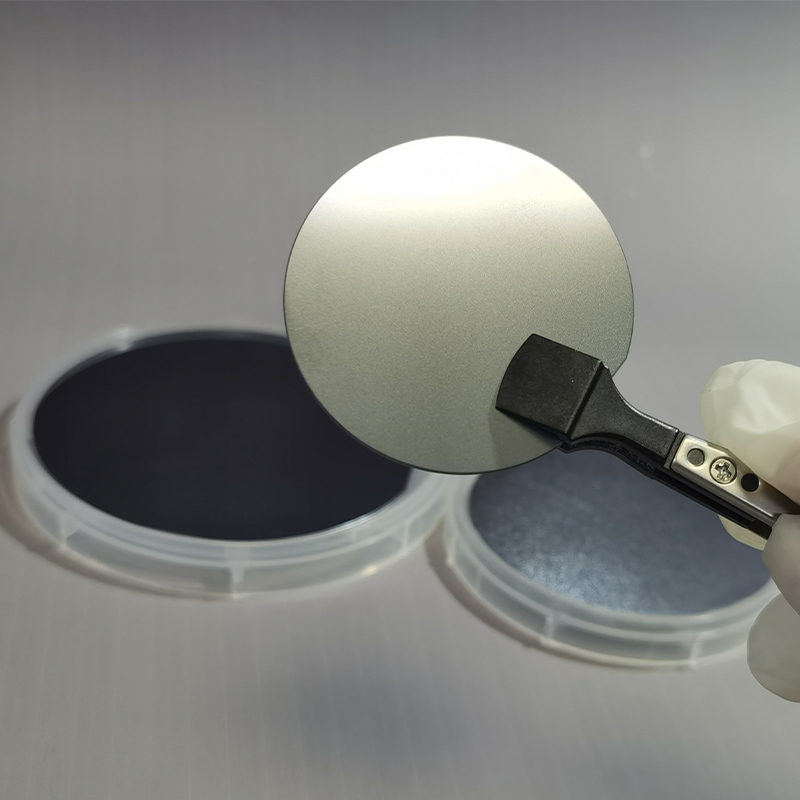
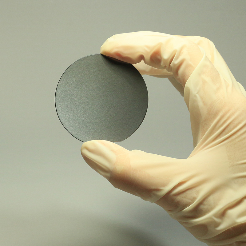
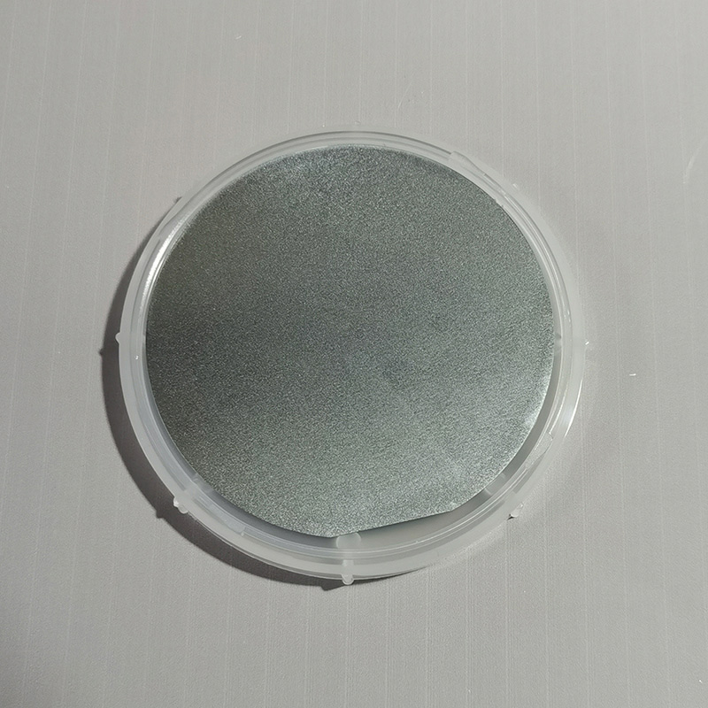
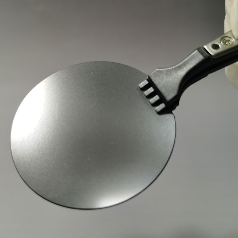
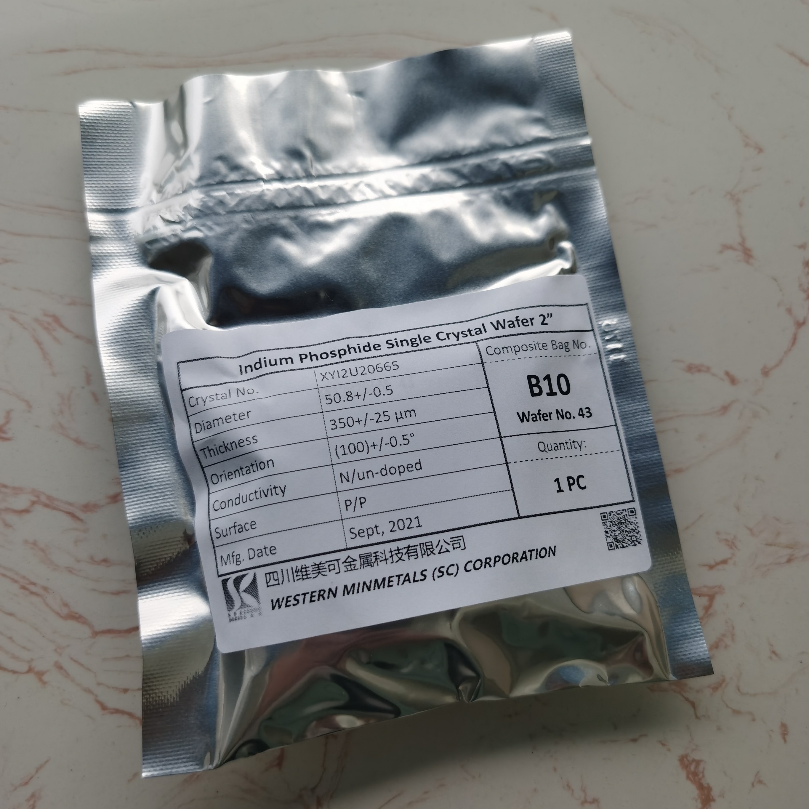
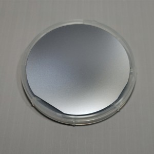
Indium Phosphide Single Crystal Wafer (InP crystal ingot or Wafer) at Western Minmetals (SC) Corporation can be offered with p-type, n-type and semi-insulating conductivity in size of 2” 3” 4” and 6”(up to 150mm) diameter, orientation <111> or <100> and thickness 350-625um with surface finish of etched and polished or Epi-ready process.
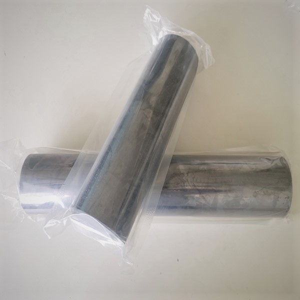
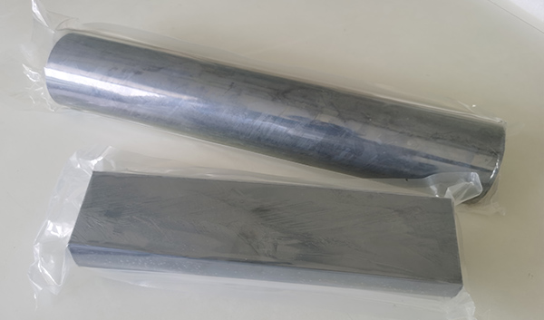
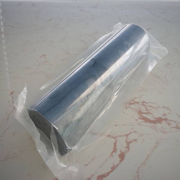
Indium Phosphide Polycrystalline or Multi-Crystal ingot (InP poly ingot) in size of D(60-75) x L(180-400) mm of 2.5-6.0kg with carrier concentration of less than 6E15 or 6E15-3E16 is available. Any customized specification available upon request to achieve the perfect solution.
| No. | Items | Standard Specification | ||
| 1 | Indium Phosphide Single Crystal | 2" | 3" | 4" |
| 2 | Diameter mm | 50.8±0.5 | 76.2±0.5 | 100±0.5 |
| 3 | Growth Method | VGF | VGF | VGF |
| 4 | Conductivity | P/Zn-doped, N/(S-doped or un-doped), Semi-insulating | ||
| 5 | Orientation | (100)±0.5°, (111)±0.5° | ||
| 6 | Thickness μm | 350±25 | 600±25 | 600±25 |
| 7 | Orientation Flat mm | 16±2 | 22±1 | 32.5±1 |
| 8 | Identification Flat mm | 8±1 | 11±1 | 18±1 |
| 9 | Mobility cm2/V.s | 50-70, >2000, (1.5-4)E3 | ||
| 10 | Carrier Concentration cm-3 | (0.6-6)E18, ≤3E16 | ||
| 11 | TTV μm max | 10 | 10 | 10 |
| 12 | Bow μm max | 10 | 10 | 10 |
| 13 | Warp μm max | 15 | 15 | 15 |
| 14 | Dislocation Density cm-2 max | 500 | 1000 | 2000 |
| 15 | Surface Finish | P/E, P/P | P/E, P/P | P/E, P/P |
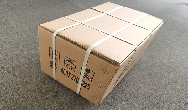
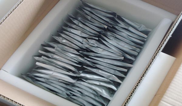
| 16 | Packing | Single wafer container sealed in aluminum composite bag. | ||
|
No. |
Items |
Standard Specification |
|
1 |
Indium Phosphide Ingot |
Poly-Crystalline or Multi-Crystal Ingot |
|
2 |
Crystal Size |
D(60-75) x L(180-400)mm |
|
3 |
Weight per Crystal Ingot |
2.5-6.0Kg |
|
4 |
Mobility |
≥3500 cm2/V.S |
|
5 |
Carrier Concentration |
≤6E15, or 6E15-3E16 cm-3 |
|
6 |
Packing |
Each InP crystal ingot is in sealed plastic bag, 2-3 ingots in one carton box. |
| Linear Formula | InP |
| Molecular Weight | 145.79 |
| Crystal structure | Zinc blende |
| Appearance | Crystalline |
| Melting Point | 1062°C |
| Boiling Point | N/A |
| Density at 300K | 4.81 g/cm3 |
| Energy Gap | 1.344 eV |
| Intrinsic resistivity | 8.6E7 Ω-cm |
| CAS Number | 22398-80-7 |
| EC Number | 244-959-5 |
Indium Phosphide InP Wafer is widely used for the manufacturing of optoelectronic components, high-power and high-frequency electronic devices, as a substrate for epitaxial indium-gallium-arsenide (InGaAs) based opto-electronic devices. Indium Phosphide is also in the fabrication for extremely promising light sources in optical fiber communications, microwave power source devices, microwave amplifiers and gate FETs devices, high-speed modulators and photo-detectors, and satellite navigation and so on.
- Sample Available Upon Request
- Safety Delivery of Goods By Courier/Air/Sea
- COA/COC Quality Management
- Secure & Convenient Packing
- UN Standard Packing Available Upon Request
- ISO9001:2015 Certified
- CPT/CIP/FOB/CFR Terms By Incoterms 2010
- Flexible Payment Terms T/T D/P L/C Acceptable
- Full Dimensional After-Sale Services
- Quality Inspection By Sate-of-the-art Facility
- Rohs/REACH Regulations Approval
- Non-Disclosure Agreements NDA
- Non-Conflict Mineral Policy
- Regular Environmental Management Review
- Social Responsibility Fulfillment


- English
- French
- German
- Portuguese
- Spanish
- Russian
- Japanese
- Korean
- Arabic
- Irish
- Greek
- Turkish
- Italian
- Danish
- Romanian
- Indonesian
- Czech
- Afrikaans
- Swedish
- Polish
- Basque
- Catalan
- Esperanto
- Hindi
- Lao
- Albanian
- Amharic
- Armenian
- Azerbaijani
- Belarusian
- Bengali
- Bosnian
- Bulgarian
- Cebuano
- Chichewa
- Corsican
- Croatian
- Dutch
- Estonian
- Filipino
- Finnish
- Frisian
- Galician
- Georgian
- Gujarati
- Haitian
- Hausa
- Hawaiian
- Hebrew
- Hmong
- Hungarian
- Icelandic
- Igbo
- Javanese
- Kannada
- Kazakh
- Khmer
- Kurdish
- Kyrgyz
- Latin
- Latvian
- Lithuanian
- Luxembou..
- Macedonian
- Malagasy
- Malay
- Malayalam
- Maltese
- Maori
- Marathi
- Mongolian
- Burmese
- Nepali
- Norwegian
- Pashto
- Persian
- Punjabi
- Serbian
- Sesotho
- Sinhala
- Slovak
- Slovenian
- Somali
- Samoan
- Scots Gaelic
- Shona
- Sindhi
- Sundanese
- Swahili
- Tajik
- Tamil
- Telugu
- Thai
- Ukrainian
- Urdu
- Uzbek
- Vietnamese
- Welsh
- Xhosa
- Yiddish
- Yoruba
- Zulu