
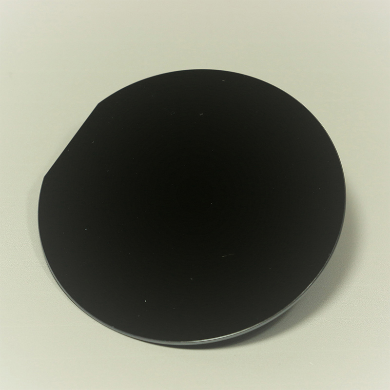
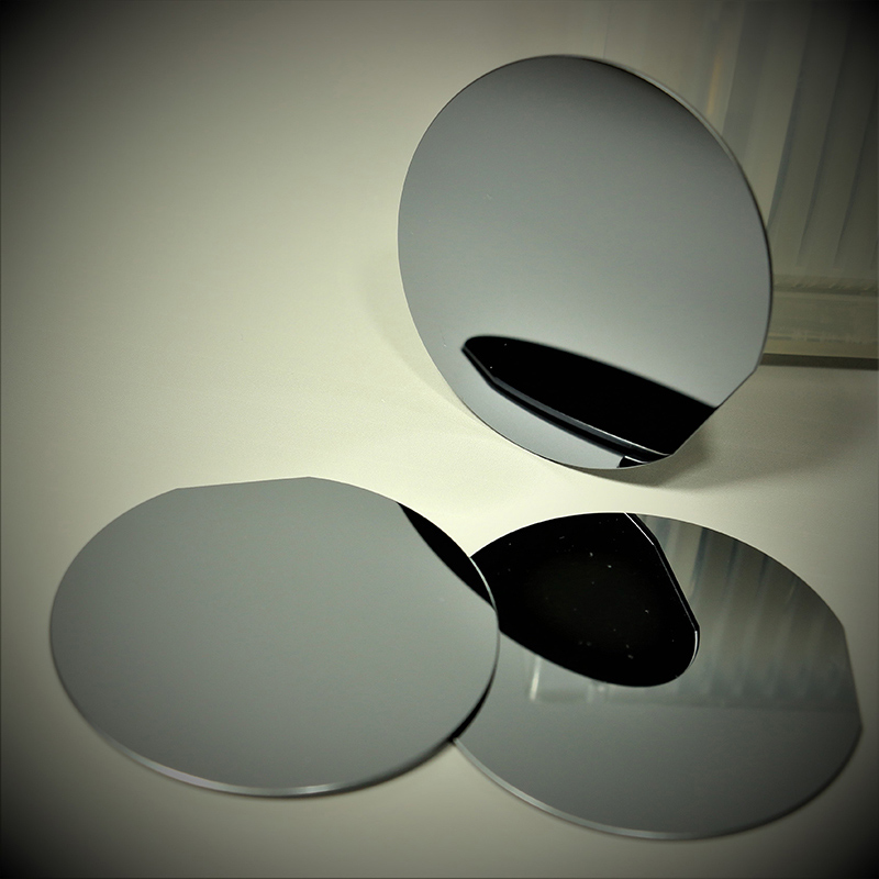
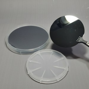
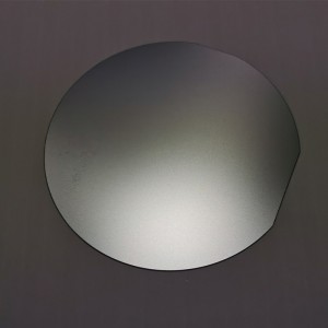
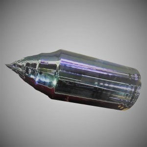
CZ Silicon Wafer
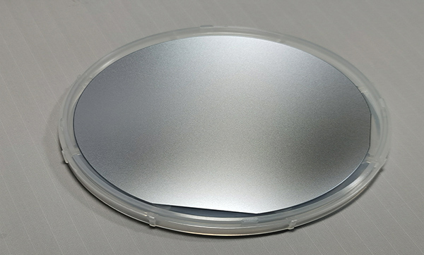
CZ Single Crystal Silicon Wafer is the basic material in the production of integrated circuits, diodes, transistors, discrete components, used in all types of electronic equipment and semiconductor devices, as well as substrate in epitaxial processing, SOI wafer substrate or semi-insulating compound wafer fabrication, especially large diameter of 200mm, 250mm and 300mm are optimal for manufacturing ultra highly integrated devices. Single Crystal Silicon is also used for solar cells in large quantities by the photovoltaic industry, which almost perfect crystal structure yields the highest light-to-electricity conversion efficiency.
| No. | Items | Standard Specification | |||||
| 1 | Size | 2" | 3" | 4" | 6" | 8" | 12" |
| 2 | Diameter mm | 50.8±0.3 | 76.2±0.3 | 100±0.5 | 150±0.5 | 200±0.5 | 300±0.5 |
| 3 | Conductivity | P or N or un-doped | |||||
| 4 | Orientation | <100>, <110>, <111> | |||||
| 5 | Thickness μm | 279, 381, 425, 525, 575, 625, 675, 725 or as required | |||||
| 6 | Resistivity Ω-cm | ≤0.005, 0.005-1, 1-10, 10-20, 20-100, 100-300 etc | |||||
| 7 | RRV max | 8%, 10%, 12% | |||||
| 8 | Primary Flat/Length mm | As SEMI standard or as required | |||||
| 9 | Secondary Flat/Length mm | As SEMI standard or as required | |||||
| 10 | TTV μm max | 10 | 10 | 10 | 10 | 10 | 10 |
| 11 | Bow & Warp μm max | 30 | 30 | 30 | 30 | 30 | 30 |
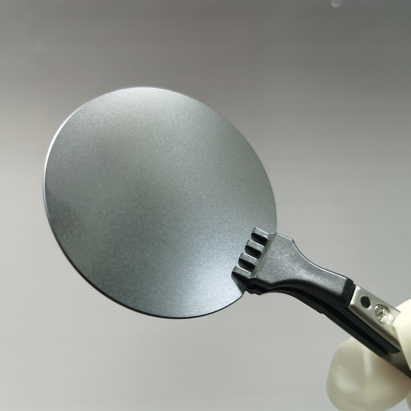
| 12 | Surface Finish | As-cut, L/L, P/E, P/P | |||||
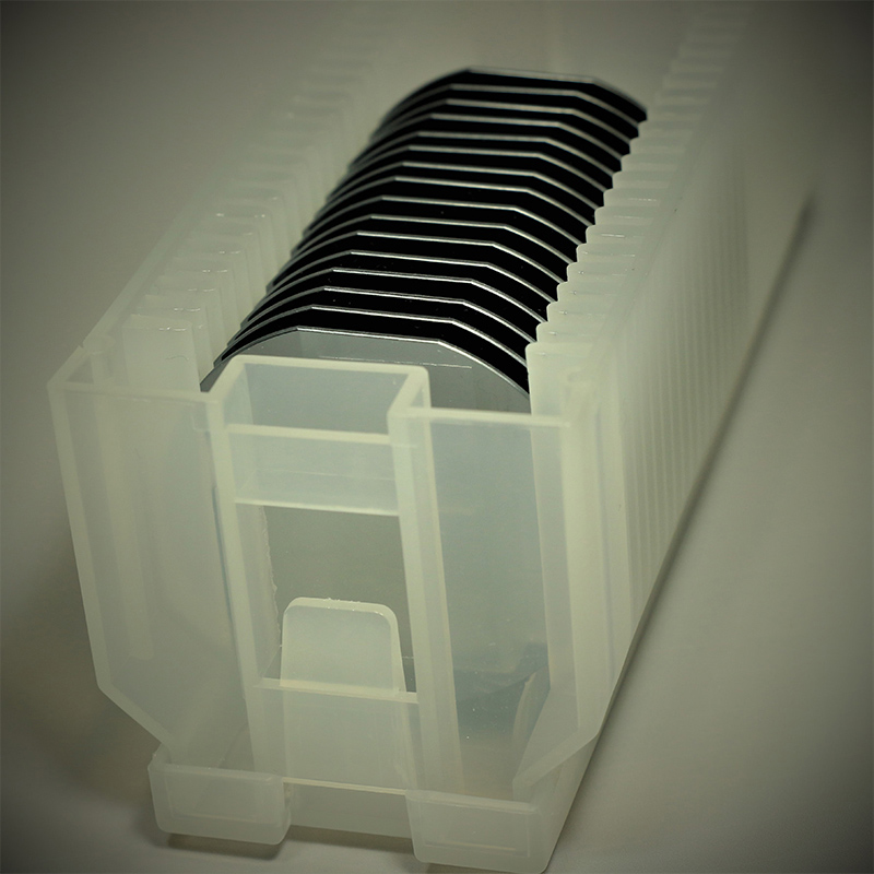
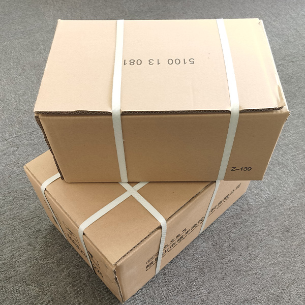
| 13 | Packing | Foam box or cassette inside, carton box outside. | |||||
| Symbol | Si |
| Atomic Number | 14 |
| Atomic Weight | 28.09 |
| Element Category | Metalloid |
| Group, Period, Block | 14, 3, P |
| Crystal structure | Diamond |
| Color | Dark gray |
| Melting Point | 1414°C, 1687.15 K |
| Boiling Point | 3265°C, 3538.15 K |
| Density at 300K | 2.329 g/cm3 |
| Intrinsic resistivity | 3.2E5 Ω-cm |
| CAS Number | 7440-21-3 |
| EC Number | 231-130-8 |
CZ or MCZ Single Crystal Silicon Wafer n-type and p-type conductivity at Western Minmetals (SC) Corporation can be delivered in size of 2, 3, 4, 6, 8 and 12 inch diameter (50, 75, 100, 125, 150, 200 and 300mm), orientation <100>, <110>, <111> with surface finish of as-cut, lapped, etched and polished in package of foam box or cassette with carton box outside.


- Sample Available Upon Request
- Safety Delivery of Goods By Courier/Air/Sea
- COA/COC Quality Management
- Secure & Convenient Packing
- UN Standard Packing Available Upon Request
- ISO9001:2015 Certified
- CPT/CIP/FOB/CFR Terms By Incoterms 2010
- Flexible Payment Terms T/T D/P L/C Acceptable
- Full Dimensional After-Sale Services
- Quality Inspection By Sate-of-the-art Facility
- Rohs/REACH Regulations Approval
- Non-Disclosure Agreements NDA
- Non-Conflict Mineral Policy
- Regular Environmental Management Review
- Social Responsibility Fulfillment


- English
- French
- German
- Portuguese
- Spanish
- Russian
- Japanese
- Korean
- Arabic
- Irish
- Greek
- Turkish
- Italian
- Danish
- Romanian
- Indonesian
- Czech
- Afrikaans
- Swedish
- Polish
- Basque
- Catalan
- Esperanto
- Hindi
- Lao
- Albanian
- Amharic
- Armenian
- Azerbaijani
- Belarusian
- Bengali
- Bosnian
- Bulgarian
- Cebuano
- Chichewa
- Corsican
- Croatian
- Dutch
- Estonian
- Filipino
- Finnish
- Frisian
- Galician
- Georgian
- Gujarati
- Haitian
- Hausa
- Hawaiian
- Hebrew
- Hmong
- Hungarian
- Icelandic
- Igbo
- Javanese
- Kannada
- Kazakh
- Khmer
- Kurdish
- Kyrgyz
- Latin
- Latvian
- Lithuanian
- Luxembou..
- Macedonian
- Malagasy
- Malay
- Malayalam
- Maltese
- Maori
- Marathi
- Mongolian
- Burmese
- Nepali
- Norwegian
- Pashto
- Persian
- Punjabi
- Serbian
- Sesotho
- Sinhala
- Slovak
- Slovenian
- Somali
- Samoan
- Scots Gaelic
- Shona
- Sindhi
- Sundanese
- Swahili
- Tajik
- Tamil
- Telugu
- Thai
- Ukrainian
- Urdu
- Uzbek
- Vietnamese
- Welsh
- Xhosa
- Yiddish
- Yoruba
- Zulu