
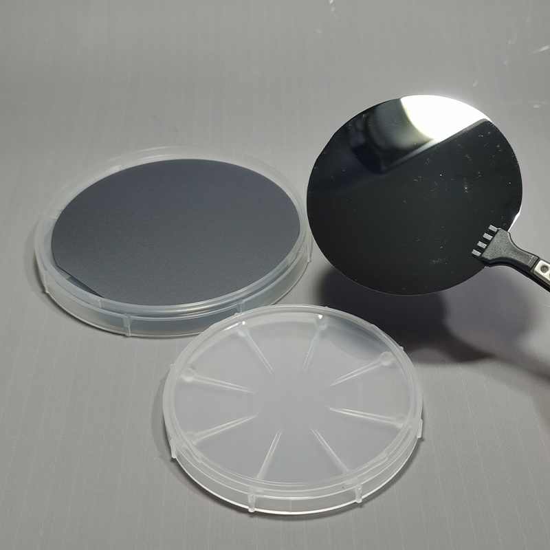
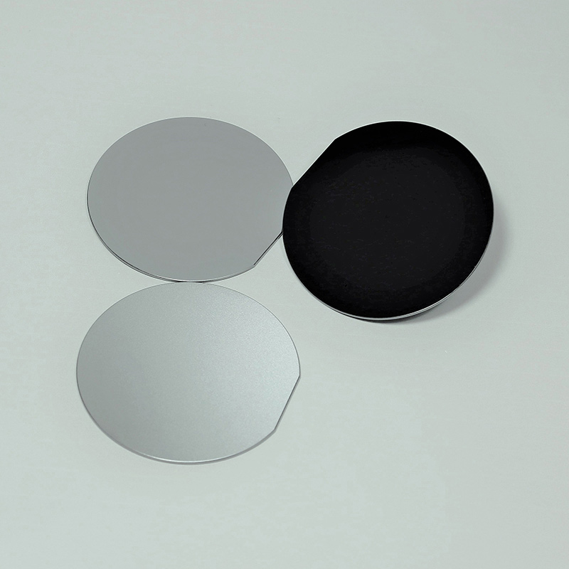
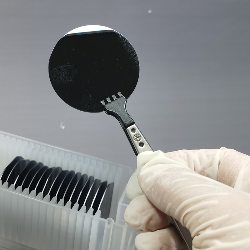
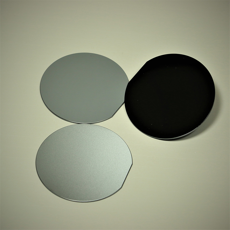
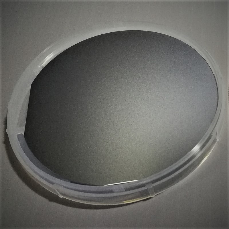
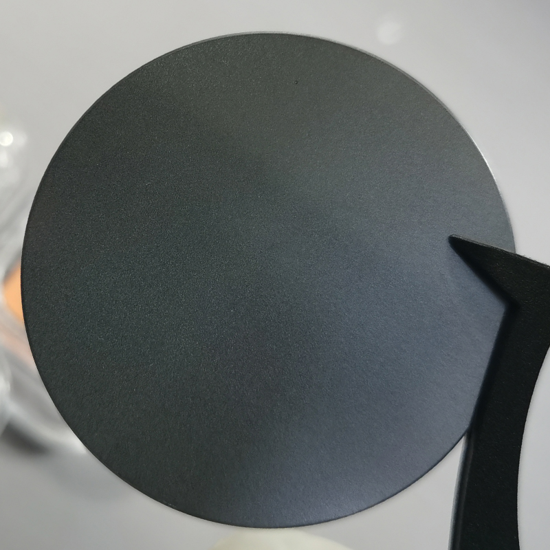
FZ Single Crystal Silicon Wafer or FZ Mono-crystal Silicon Wafer of intrinsic, n-type and p-type conductivity at Western Minmetals (SC) Corporation can be delivered in various size of 2, 3, 4, 6 and 8 inch in diameter (50mm, 75mm, 100mm, 125mm, 150mm and 200mm) and wide range of thickness from 279um up to 2000um in <100>, <110>, <111> orientation with surface finish of as-cut, lapped, etched and polished in package of foam box or cassette with carton box outside.
| No. | Items | Standard Specification | ||||
| 1 | Size | 2″ | 3″ | 4″ | 5″ | 6″ |
| 2 | Diameter mm | 50.8±0.3 | 76.2±0.3 | 100±0.5 | 125±0.5 | 150±0.5 |
| 3 | Conductivity | N/P | N/P | N/P | N/P | N/P |
| 4 | Orientation | <100>, <110>, <111> | ||||
| 5 | Thickness μm | 279, 381, 425, 525, 575, 625, 675, 725 or as required | ||||
| 6 | Resistivity Ω-cm | 1-3, 3-5, 40-60, 800-1000, 1000-1400 or as required | ||||
| 7 | RRV max | 8%, 10%, 12% | ||||
| 8 | TTV μm max | 10 | 10 | 10 | 10 | 10 |
| 9 | Bow/Warp μm max | 30 | 30 | 30 | 30 | 30 |
| 10 | Surface Finish | As-cut, L/L, P/E, P/P | ||||
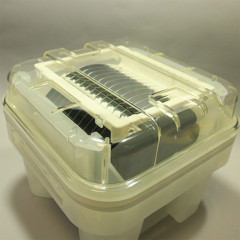
| 11 | Packing | Foam box or cassette inside, carton box outside. | ||||
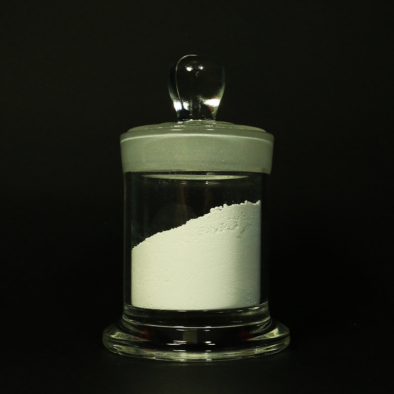
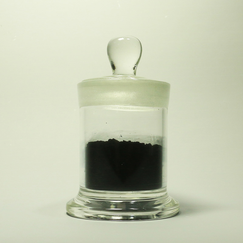
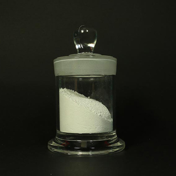
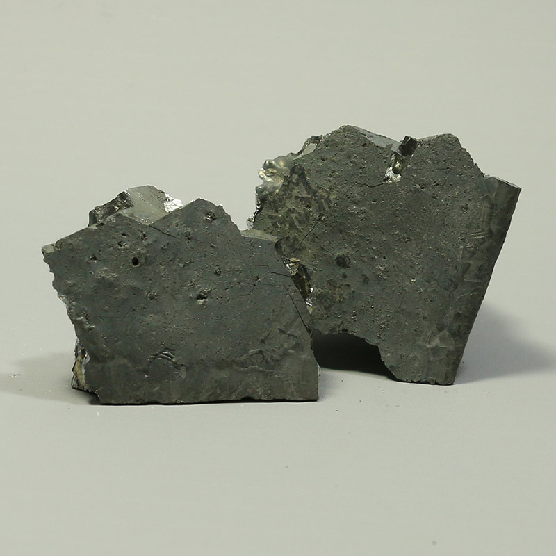
| Symbol | Si |
| Atomic Number | 14 |
| Atomic Weight | 28.09 |
| Element Category | Metalloid |
| Group, Period, Block | 14, 3, P |
| Crystal structure | Diamond |
| Color | Dark gray |
| Melting Point | 1414°C, 1687.15 K |
| Boiling Point | 3265°C, 3538.15 K |
| Density at 300K | 2.329 g/cm3 |
| Intrinsic resistivity | 3.2E5 Ω-cm |
| CAS Number | 7440-21-3 |
| EC Number | 231-130-8 |
- Sample Available Upon Request
- Safety Delivery of Goods By Courier/Air/Sea
- COA/COC Quality Management
- Secure & Convenient Packing
- UN Standard Packing Available Upon Request
- ISO9001:2015 Certified
- CPT/CIP/FOB/CFR Terms By Incoterms 2010
- Flexible Payment Terms T/T D/P L/C Acceptable
- Full Dimensional After-Sale Services
- Quality Inspection By Sate-of-the-art Facility
- Rohs/REACH Regulations Approval
- Non-Disclosure Agreements NDA
- Non-Conflict Mineral Policy
- Regular Environmental Management Review
- Social Responsibility Fulfillment