


|
No. |
Item |
Standard Specification |
||
|
Formula |
Purity |
Impurity PPM Max each |
||
|
1 |
Antimony Selenide |
Sb2Se3 |
4N 5N |
Available Upon Request. Special specification can be customized |
|
2 |
Arsenic Selenide |
As2Se3 |
4N 5N |
|
|
3 |
Bismuth Selenide |
Bi2Se3 |
4N 5N |
|
|
4 |
Cadmium Selenide |
CdSe |
4N 5N 6N |
|
|
5 |
Copper Selenide |
CuSe |
4N 5N |
|
|
6 |
Gallium Selenide |
Ga2Se3 |
4N 5N |
|
|
7 |
Indium Selenide |
In2Se3 |
4N 5N |
|
|
8 |
Lead Selenide |
PbSe |
4N |
|
| 9 | Molybdenum Selenide |
MoSe2 |
4N 5N |
|
|
10 |
Tin Selenide |
SnSe |
4N 5N |
|
|
11 |
Tungsten Selenide |
WSe2 |
3N 4N |
|
|
12 |
Zinc Selenide |
ZnSe |
4N 5N |
|
|
13 |
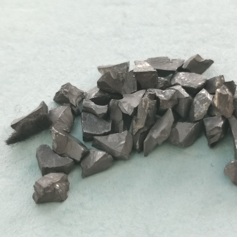
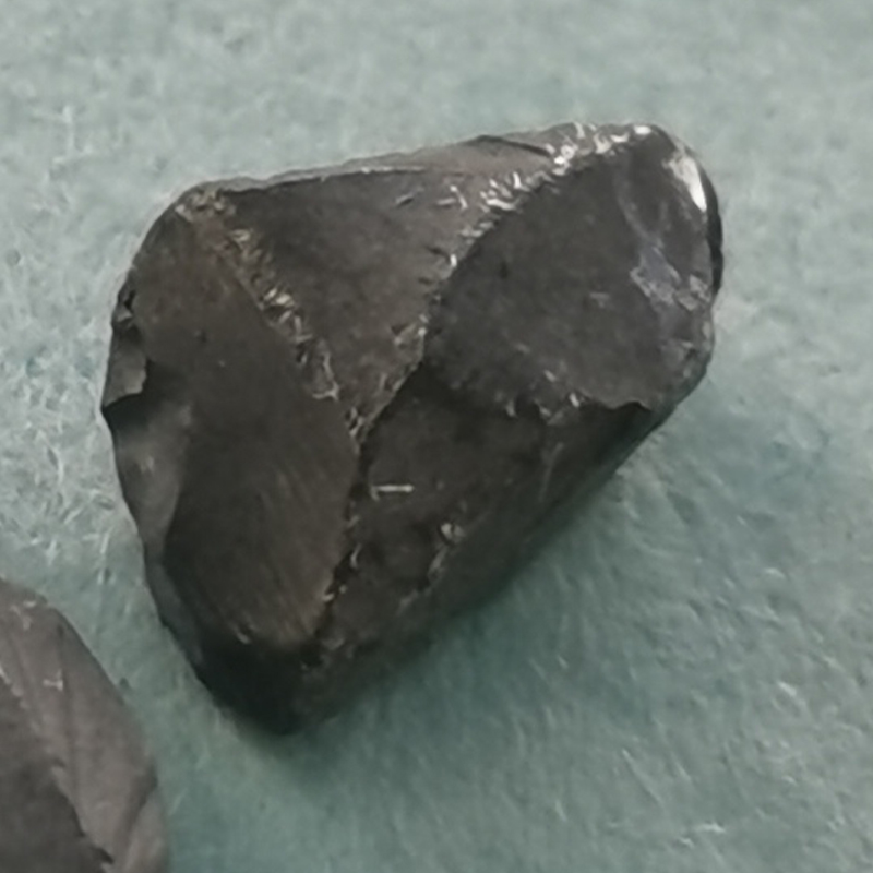
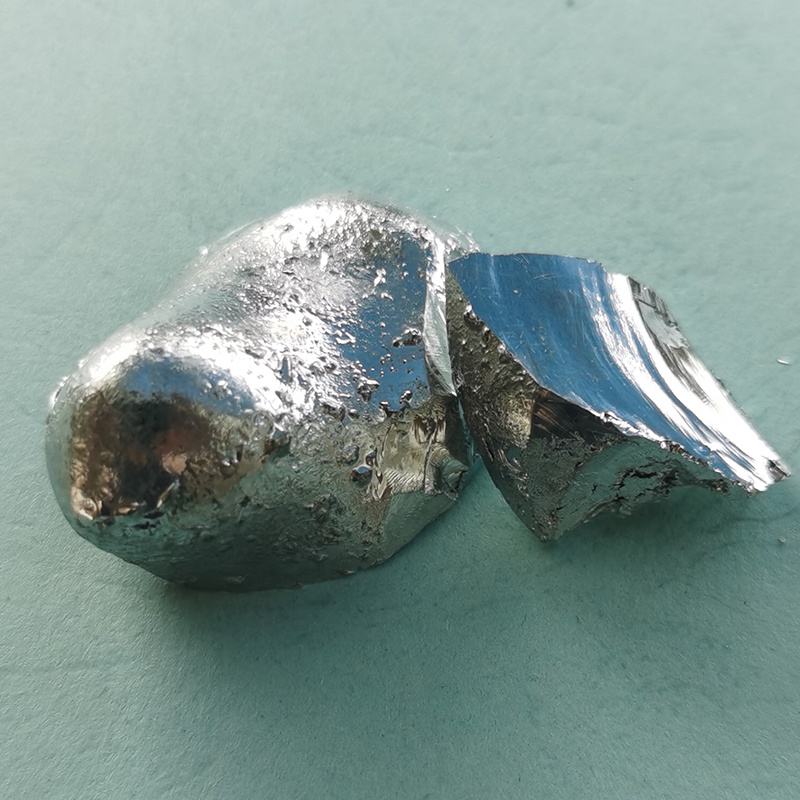
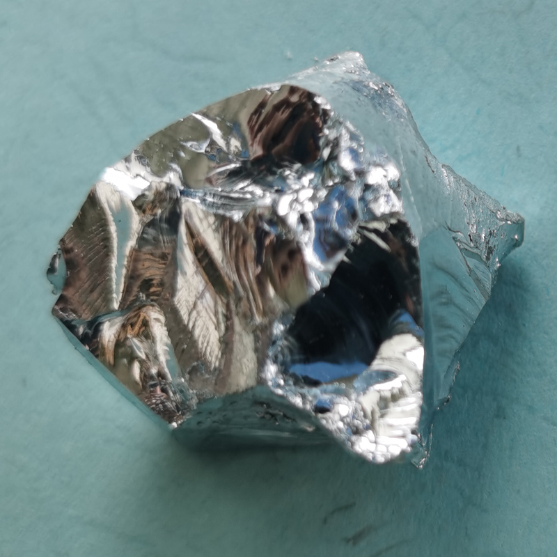
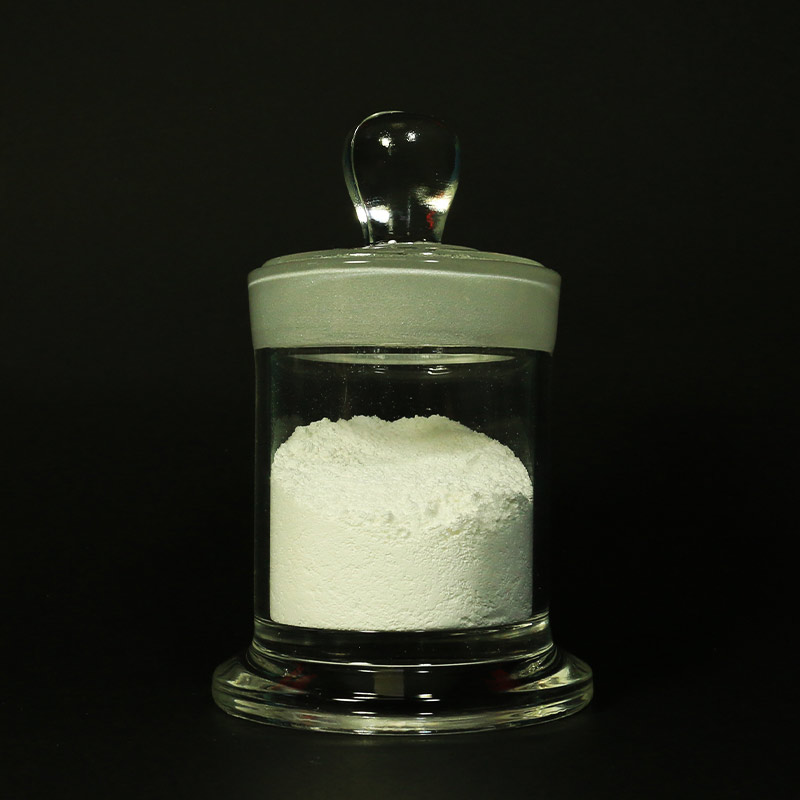
Size |
-60/-80mesh, 1-20mm Lump, 1-6mm Granule, Target or Blank |
||
|
14 |
Packing |
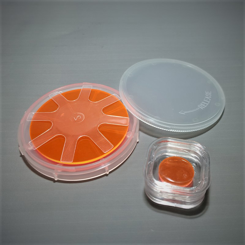
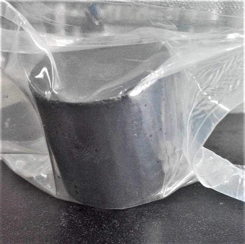
In polyethylene bottle or composite bag, 1kg each. |
||
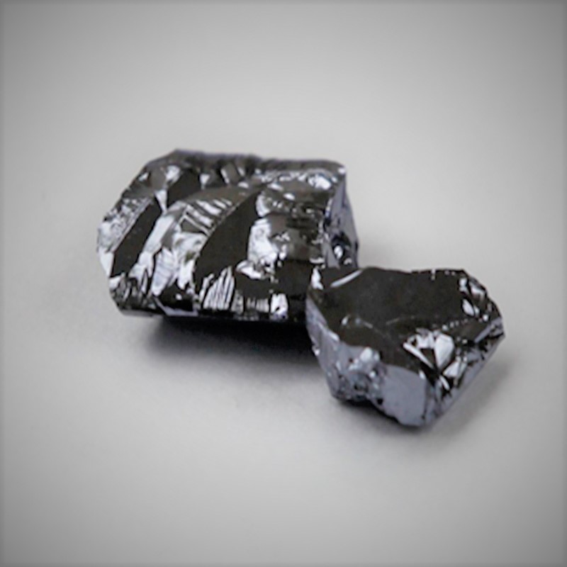
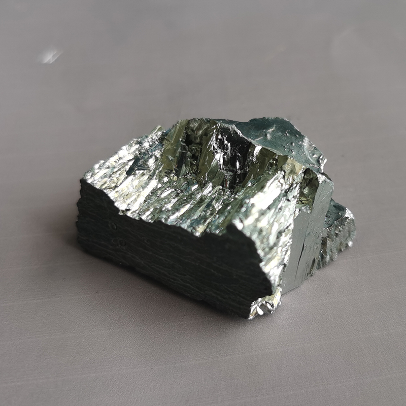
Antimony Selenide Sb2Se3, a kind of inorganic compound, binary single-phase compound semiconductor, CAS 1315-05-5, MW 480.4, density 5.843g/cm3, melting point of 611oC, very slightly soluble in water, is synthesized by Bridgman method and flux zone technique. With suitable energy band gap, high absorption coefficient, simple phase and low crystallization temperature, Antimony Selenide is a economic, non-toxicity and stable inorganic thin film solar cell material. Antimony Selenide Sb2Se3 crystal exhibits topological insulator state, superconductivity, high thermoelectric efficiency, ideal environmental stability and high crystalline order, which has applications in thermoelectric, photovoltaic and optical storage. Bulk material under high pressure becomes a topological insulator and further undergoes insulator to metal to superconducting transitions. Various methods employed for the preparations of crystalline Sb2Se3 thin film, including spray pyrolysis, solution growth, direct fusion of antimony and selenium, electrochemical deposition and vacuum evaporation, Sb2Se3 can be synthesized in different types of nanostructures which exhibits direct band gaps, whereas the bulk has an indirect energy band gap of 1.21 eV. Antimony Selenide single crystal, a layer-structured direct bandgap semiconductor with orthorhombic crystal structure, has received a great deal of attention due to its switching effects and excellent photovoltaic and thermoelectric properties. Sb2Se3 photodetectors show excellent photoelectric performance, mid-infrared frequency conversion, and nonlinear applications. Antimony Selenide Sb2Se3 at Western Minmetals (SC) Corporation with purity of 99.99% 4N, 99.999% 5N can be delivered in form of powder, granule, lump, chunk, blank, bulk crystal and single crystal etc or as customized specification.
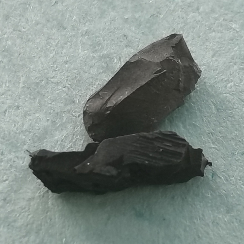
Arsenic Selenide or Arsenic Triselenide As2Se3, CAS 1303-36-2, molecular weight 386.72, density 4.75g/cm3, melting point 360°C, black or dark brown solid crystalline solid, is an inorganic chemical compound, a selenide of arsenic, is soluble in nitric acid but insoluble in water. Arsenic Selenide compound is prepared by using metaarsenite and amorphous selenium in organic medium, through heating the stoichiometric ratio As and Se in vacuum quartz ampoule to get As2Se3. The synthetic crystal of Arsenic triselenide is grown by vapour phase technique. Single crystals of As2Se3 can be prepared hydrothermally. Amorphous Arsenic Selenide is used as a vacuum deposition, chalcogenide glass for infrared optics. Due to its high refractive index, mid-IR transparency and high non-linear optical indices, thin film Arsenic Selenide is an important material for integrated photonics, semiconductor and in photo optic applications. Besides, its bandgap of 1.8 eV and wide transmission window makes it useful for applications in the shortwave infrared into the long-wave infrared. Meanwhile, Arsenic Selenide is an important raw material and intermediate used in organic synthesis, pharmaceuticals industry. Arsenic Selenide As2Se3 at Western Minmetals (SC) Corporation with purity of 99.99% 4N, 99.999% 5N can be delivered in form of powder, granule, lump, chunk, blank, bulk crystal and single crystal etc or as customized specification.
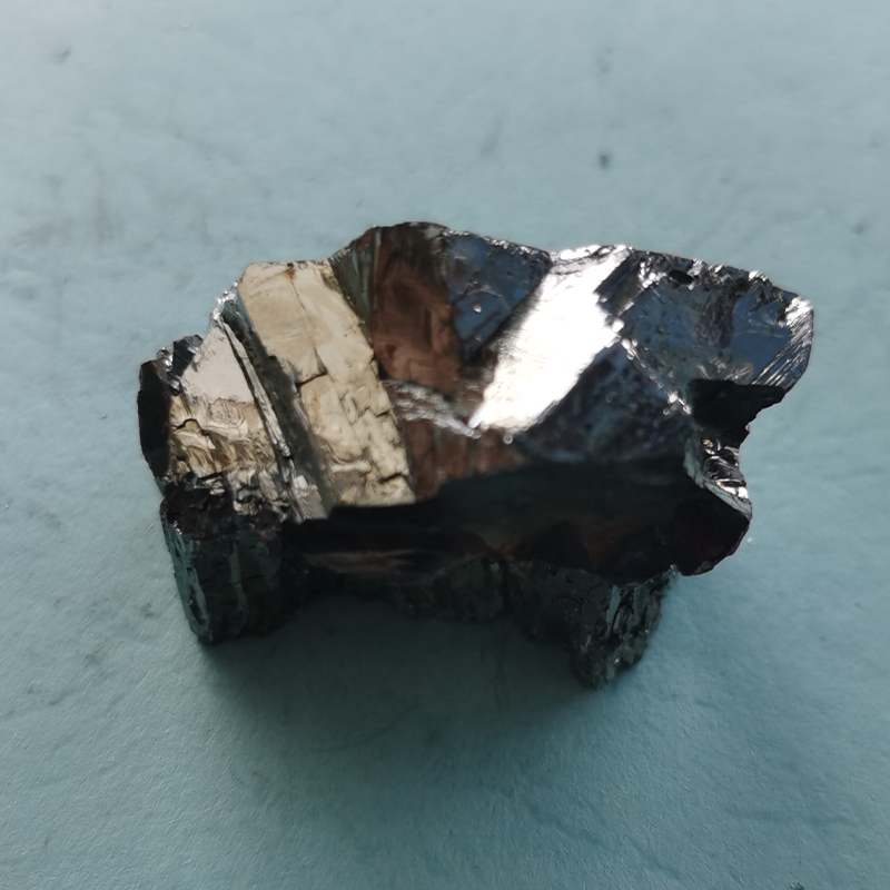
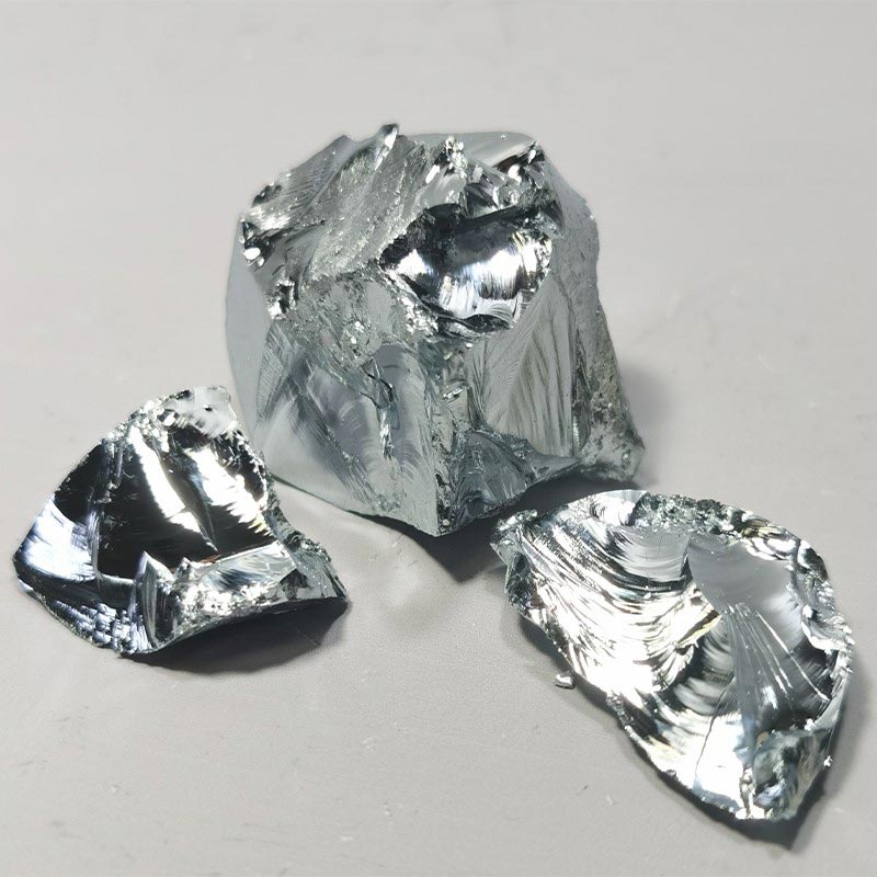
Bismuth Selenide Bi2Se3, black crystal appearance, CAS 12068-69-8, MW 654.84, melting point 710°C, boiling point 1007°C, density 6.82g/cm3, rhomb and hexagonal Structure, is insoluble in water and organic solvents. but soluble in strong acids, decomposes when heated in air, and decomposes in nitric acid and aqua regia. Bismuth selenide Bi2Se3 belongs to group 15 (VA) post-transition metal trichalcogenides, which is predicted to be 3D strong topological insulator with topologically non-trivial energy gap of 0.3 eV. Bismuth Selenide crystal is an indirect band gap semiconductor synthesized by hydrothermal method, Bridgeman R, direct method and zone floating method etc, the synthesized material is utilized to deposit bismuth selenide thin film at various substrate temperatures. Polycrystalline stoichiometric Bi2Se3 thin film is of N-type and carrier concentration of 1.02×1019 cm-3 at room temperature. Bismuth selenide powder is suitable for liquid chemical exfoliation to prepare Bi2Se3 nanosheets and nanoparticles. Bulk single Bismuth Selenide crystal is most commonly used as source from which single or few-layer sheets can be obtained by mechanical or liquid exfoliation. With remarkable thermoelectric and photoelectric properties, Bismuth selenide finds application in advanced photodetectors, magnetic devices, FETs, lasers, sputtering target, gas sensors, thermoelectric material, thin film solar cells, and quantum computing devices, Bismuth Selenide Bi2Se3 is also attractive to biomedicine due to the good bioactivity and biocompatibility. Bismuth Selenide Bi2Se3 at Western Minmetals (SC) Corporation with purity of 99.99% 4N, 99.995% 4N5, 99.999% 5N can be delivered in form of powder, granule, lump, chunk, blank, bulk crystal and single crystal etc or as customized specification.
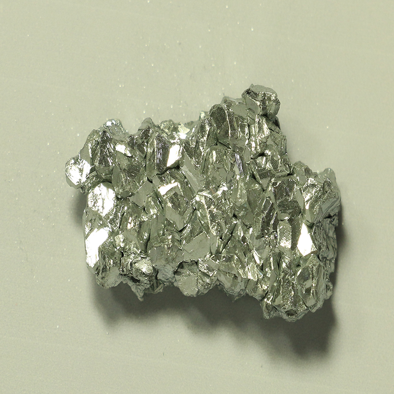
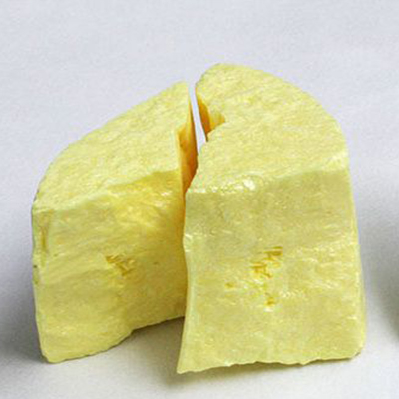
Cadmium Selenide CdSe, red to black crystal, most common Wurtzite hexagonal structure, CAS 1306-24-7, molecular weight 191.377, density 5.8g/cm3, melting point 1350°C, insoluble in Water, is a solid, binary primarily ionic compound of cadmium and selenium. Polycrystalline compounds is synthesized by the High-Pressure Vertical Bridgman method or High-Pressure Vertical Zone Melting, or distillation and CVD synthesis, which is used for growing CdSe single crystal, CdSe evaporation material, namely for making photocell, rectifier, luminous paint, etc. Cadmium Selenide with wurtzite crystal structure is an important II-VI n-type semiconductor, and has a band gap of 1.74 eV. CdSe nanoparticle by several production methods of arrested precipitation in solution, synthesis in structured media, high temperature pyrolysis, sonochemical, and radiolytic methods is of 1–100 nm in size, exhibits a property known as quantum confinement, they are finding applications in opto-electronic devices such as laser diodes that cover a large part of the electromagnetic spectrum, especially useful as a component of photocatalysts, use in biomedical imaging applications, and is used in windows for instruments using infra-red (IR) light, nanosensing and high-efficiency solar cells. Cadmium Selenide CdSe at Western Minmetals (SC) Corporation with purity of 99.99% 4N, 99.999% 5N and 99.9999% 6N can be delivered in form of powder, granule, lump, chunk, blank, bulk crystal and single crystal etc or as customized specification.
Copper Selenide or Dicopper Selenide, Cuprous Selenide, CAS No 20405-64-5, black cubic crystal, density 6.749, melting point 1113°C, insoluble in water but easily soluble in nitric acid, soluble in sulfuric acid and ammonia. Copper Selenide is prepared in a vacuum quartz seal tube placed in horizontal synthesis furnace. Ligand-stabilized copper selenide (Cu(2-x)Se) nanocrystal is synthesized by a colloidal hot injection process, which readily disperse in water and exhibit strong near-infrared (NIR) optical absorption with a high molar extinction coefficient, it finds application in photothermal therapy, ad for the preparation of group compound semiconductor, cuprous selenide target material, copper-indium-gallium-Selenium CIGS thin film solar cell etc. Copper Selenide CuSe at Western Minmetals (SC) Corporation with purity of 99.99% 4N, 99.999% 5N can be delivered in form of powder, granule, lump, chunk, pill, needle, blank, bulk crystal and single crystal etc or as customized specification.
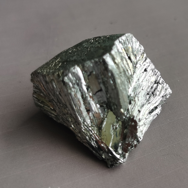
Tungsten Selenide or Tungsten Diselenide, WSe2 CAS 12067-46-8, density 9.32g/cm3, molecular weight 341.76, is insoluble in water. Tungten Diselenide belongs to group V transition metal dihaloalkanes TMDC. WSe2 is a P-type or N-type semiconductor with an indirect band gap of ~ 1.3ev, and a single layer of WSe2 has a direct band gap. These layers are stacked together by vander Waals interaction and can be stripped into thin 2D layers. Being Lamellar structured, dry and solid lubricant, WSe2 has the lowest thermal conductivity with exceptional stability at high temperatures and in high vacuum. Tungsten Selenide thin films for terrestrial photovoltaic is synthesized by Chemical-Vapor-Deposition CVD, which can be for flexible thin film solar cell, or as a sputtering target. Tungsten Selenide WSe2 at Western Minmetals (SC) Corporation with purity of 99.99% 4N, 99.999% 5N and 99.9999% 6N can be delivered in form of powder, granule, lump, chunk, blank, target, bulk crystal etc or as customized specification.
Gallium Selenide or Gallium Triselenide Ga2Se3, CAS 12024-11-2, molecular mass148.68, melting point 960°C density 5.030g/cm3, a dark brown, shiny flake crystal with hexagonal structure, is a compound of Gallium and Selenium by chemical vapor deposition CVD method. GaSe is a layered semiconductor belongs to the family of metal chalcogens that crystallize in a layered structure. With the decrease of temperature, the maximum value of photoelectric effect of GaSe moves to the direction of short wave. Gallium Selenide GaSe crystal can be synthesized through different growth techniques of Bridgman growth, chemical vapor transport CVT and flux zone growth to optimize grain sizes and reduce defect concentrations. Gallium selenide GaSe crystal is proposed as the active compound for use in photovoltaic devices suited towards electronic and optical applications in 2D materials field, as intercalation electrodes in electrochemical lithium cells, and as a nonlinear optical medium. Gallium Selenide Ga2Se3 at Western Minmetals (SC) Corporation with purity of 99.99% 4N, 99.999% 5N can be delivered in form of powder, granule, lump, chunk, blank, bulk crystal and single crystal etc or as customized specification.
Indium Selenide, or Diinsium Triselenide In2Se3, black to dull grease luster powder or lump, CAS No 2056-07-4, melting point 660°C, density 5.55g/cm3, is a compound of indium and selenium, which is stable under room temperature and pressure, and kept to avoid light, open fire and high temperature. It is soluble in strong acid and easy to decompose. The semiconductive compound In2Se3 has a defective ZnS lattice structure in which the non-metallic atoms are arranged in tetrahedron by three metal atoms and one vacancy. To ensure structural, optical, and electronic consistency, Indium Selenide or Diindium Triselenide InSe is developed by Brigmann method preferable to offer highly crystallization as well as large size. Besides, the Flux Zone Growth and Chemical Vapor Transport CVT growth techniques are also optional. In2Se3 crystal is a direct gap semiconductor of 1.56eV emission (300K), α- In2Se3 and β- In2Se3 crystals are the two most common forms with defect wurtzite structures. It is mainly used as semiconductor, optical materials, photovoltaic devices, electrical sensors, or to be used for preparing copper indium gallium selenium CIGS thin film material. Indium Selenide InSe at Western Minmetals (SC) Corporation with 99.99% 4N, 99.999% 5N purity can be delivered in form of powder, granule, lump, chunk, blank, bulk crystal etc or as customized specification.
Lead Selenide PbSe, gray or grayish black crystalline solid, a selenide of lead, cubic crystal of the NaCl structure, CAS 12069-00-0, MW 286.16,density 8.10g/cm3, melting 1078°C, is insoluble in water but soluble in nitric acid and hot concentrated hydrochloric acid. Lead Selenide is prepared by mixing high-purity lead and selenium in stoichiometric proportion and heating them in quartz ampoules to 1100-1150° in furnace or reduction of lead selenite with hydrogen. Lead selenide is a semiconductor material of direct bandgap of 0.27 eV at room temperature, which performs efficiently at low temperatures without the need for cooling. As a sensitive material to the infrared radiation, PbSe has unique and outstanding characteristics making this material an excellent detector of low cost high speed infrared imagers for thermal imaging operating at wavelengths between 1.5–5.2μm, and to make photosensitive resistance. Lead selenide nanocrystal can be used as quantum dots, for example in nanocrystal solar cells. Meanwhile, Lead Selenide is a high performance thermoelectric material which has a number of industrial applications. Lead Selenide PbSe at Western Minmetals (SC) Corporation with purity of 99.99% 4N can be delivered in form of powder, granule, lump, chunk, blank, bulk crystal and single crystal etc or as customized specification.
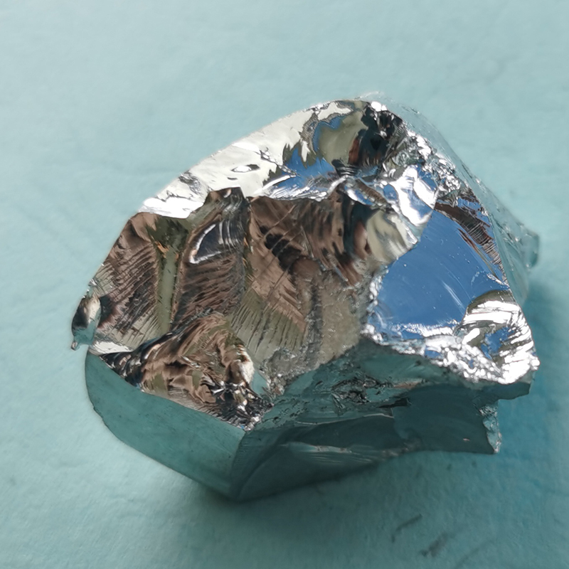
Molybdenum Selenide MoSe2, gray solid crystalline appearance, layered structure, is an inorganic compound semiconductor of molybdenum and selenium, which is known as group VI transition metal dichalcofemides, CAS 12058-18-3, density 6.0g/cm3, MW 253.86, melting point 1200°C, insoluble in water. Bulk MoSe synthesis and purification involves direct reaction of molybdenum and selenium by chemical vapor transport CVT, singlr crytstal MoSe is produced by scotch tape exfoliation from bulk crystal or by chemical vapor deposition CVD. Molybdenum Selenide MoSe2, narrow band gap of 1.2ev, can not only absorb ultraviolet light but also visible light, it exhibits a wide range of light response and high utilization efficiency of solar light, so it is used as photodetectors and transistors. Molybdenum Selenide’s layered nature and higher electrical conductivity gives rise to several interesting applications such as field effect transistors, piezoelectrics, and substrates for self assembly, and also for material modification, lubricant additives, solar cells, energy storage, microelectronics, optoelectronics and high performance photocatalysts. Molybdenum Selenide MoSe2 at Western Minmetals (SC) Corporation with purity of 99.99% 4N can be delivered in form of submicro and nanomicron powder, granule, lump, chunk, blank, bulk crystal and single crystal etc or as customized specification.
Tin Selenide SnSe, gray solid crystal with rhombic crystal structure, molecular weight 199.68, density 6.18g/cm3, melting point 861°C, can be dissolved in alkali metal sulfide and selenide, and easily soluble in nitric acid and aqua regia but insoluble in water. SnSe compound is typical layered material synthesized by the various methods employed for the phase-pure SnSe like hot injection, facile surfactant-free synthesis, thermal evaporation, insert gas condensation etc. Tin Selenide is an important IV-VI semiconductor, the indirect band gap of bulk materials is 0.90 EV and the direct band gap is 1.30 eV, which can absorb most of the solar spectrum, and been extensively explored in the thermoelectric fields and photovoltaic PV application for its extraordinary advantages including excellent optoelectronic properties, absence of toxicity, economically raw material, relative abundance, environmental friendliness and chemical stability. As tin-based binary chalcogenide compound, the electronic, thermoelectric, and optoelectronic characteristics of bulk crystals, thin films, and nanostructures of Tin Selenide SnSe finds novel applications in the next generation electronic, optical, optoelectronic, flexible systems, Li-ion rechargeable batteries, super capacitors, phase-change memory devices and topological insulators. Tin Selenide SnSe at Western Minmetals (SC) Corporation with purity of 99.99% 4N, 99.999% 5N can be delivered in form of powder, granule, lump, chunk, blank, bulk crystal and single crystal etc or as customized specification.
- Sample Available Upon Request
- Safety Delivery of Goods By Courier/Air/Sea
- COA/COC Quality Management
- Secure & Convenient Packing
- UN Standard Packing Available Upon Request
- Quality Inspection Including XRD/SEM/ICP/GDMS etc
- Full Scope of Trade Terms CPT/FOB/ CFR/CIP By Incoterms 2010
- Flexible Payment Terms T/T D/P L/C Acceptable
- Full Dimensional After-Sale Services
- ISO9001:2015 Certified & Rohs/REACH Regulations Approval
- Non-Disclosure Agreements
- Non-Conflict Mineral Policy
- Regular Environmental Management Review
- Social Responsibility Fulfillment
