
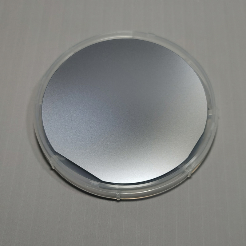

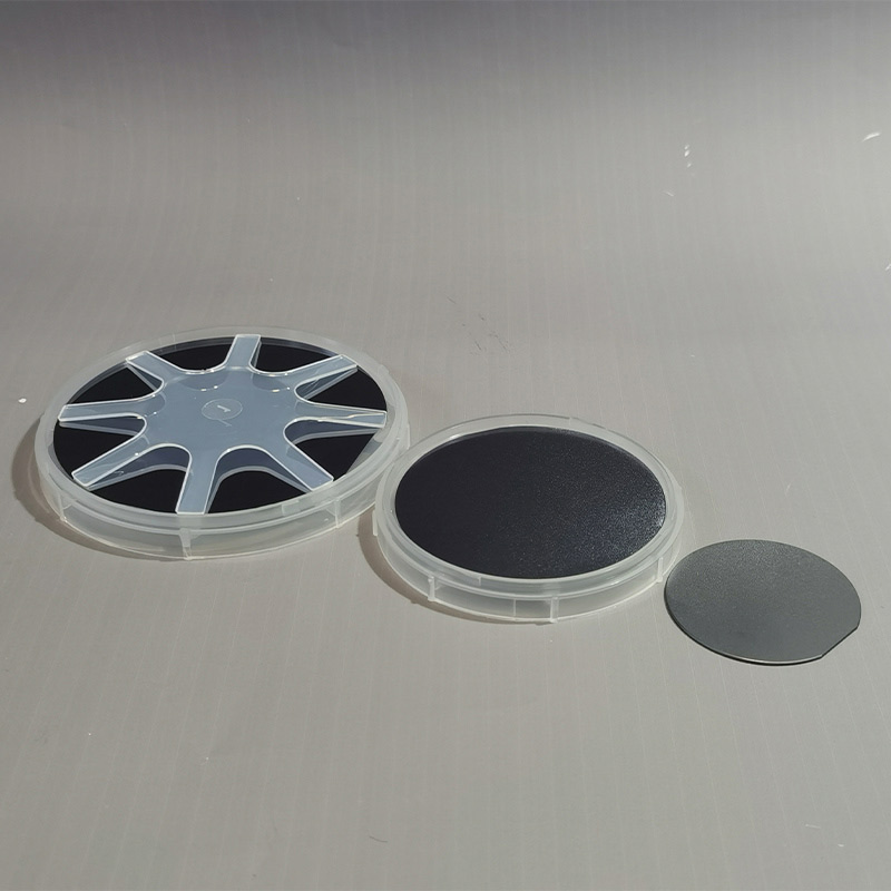

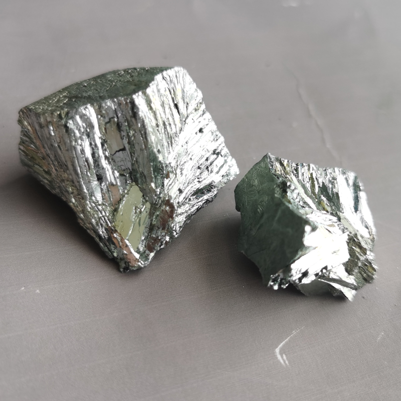
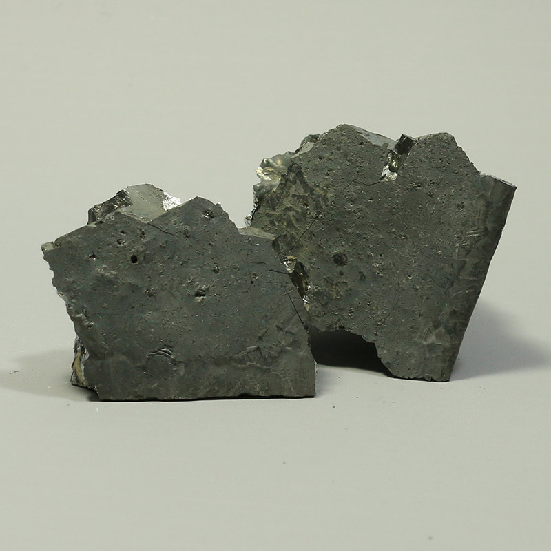
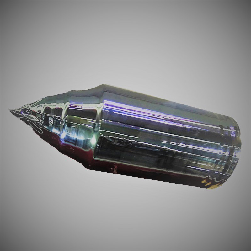
Gallium Antimonide GaSb substrate is being utilized in the most cutting-edge photo-optic and optoelectronic applications such as the fabrications of photo detectors, infrared detectors with long life, high sensitivity and reliability, photoresist component, infrared LEDs and lasers, transistors, thermal photovoltaic cell and thermo-photovoltaic systems.
| Linear Formula | GaSb |
| Molecular Weight | 191.48 |
| Crystal structure | Zinc blende |
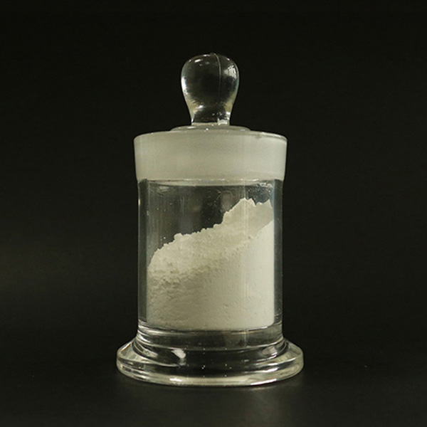
| Appearance | Gray crystalline solid |
| Melting Point | 710°C |
| Boiling Point | N/A |
| Density at 300K | 5.61 g/cm3 |
| Energy Gap | 0.726 eV |
| Intrinsic resistivity | 1E3 Ω-cm |
| CAS Number | 12064-03-8 |
| EC Number | 235-058-8 |
| No. | Items | Standard Specification | ||
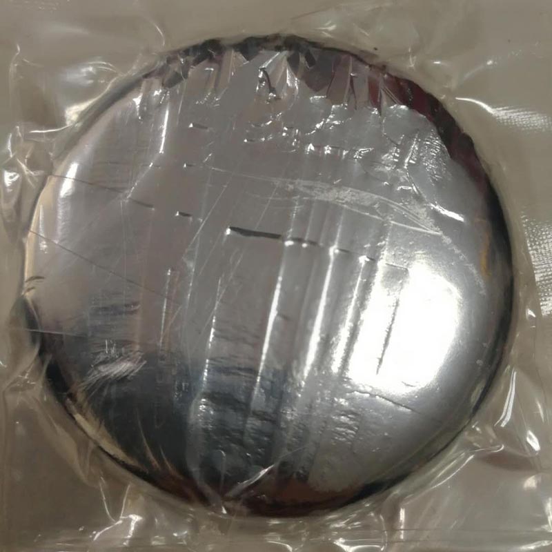
| 1 | Size | 2″ | 3″ | 4″ |
| 2 | Diameter mm | 50.5±0.5 | 76.2±0.5 | 100±0.5 |
| 3 | Growth Method | LEC | LEC | LEC |
| 4 | Conductivity | P-type/Zn-doped, Un-doped, N-type/Te-doped | ||
| 5 | Orientation | (100)±0.5°, (111)±0.5° | ||
| 6 | Thickness μm | 500±25 | 600±25 | 800±25 |
| 7 | Orientation Flat mm | 16±2 | 22±1 | 32.5±1 |
| 8 | Identification Flat mm | 8±1 | 11±1 | 18±1 |
| 9 | Mobility cm2/V.s | 200-3500 or as required | ||
| 10 | Carrier Concentration cm-3 | (1-100)E17 or as required | ||
| 11 | TTV μm max | 15 | 15 | 15 |
| 12 | Bow μm max | 15 | 15 | 15 |
| 13 | Warp μm max | 20 | 20 | 20 |
| 14 | Dislocation Density cm-2 max | 500 | 1000 | 2000 |
| 15 | Surface Finish | P/E, P/P | P/E, P/P | P/E, P/P |
| 16 | Packing | Single wafer container sealed in Aluminum bag. | ||
- Sample Available Upon Request
- Safety Delivery of Goods By Courier/Air/Sea
- COA/COC Quality Management
- Secure & Convenient Packing
- UN Standard Packing Available Upon Request
- Quality Inspection Including XRD/SEM/ICP/GDMS…
- Full Scope of Trade Terms CPT/CIP/FOB/CFR By Incoterms 2010
- Flexible Payment Terms T/T D/P L/C Acceptable
- Full Dimensional After-Sale Services
- ISO9001:2015 Certified
- Rohs & REACH Regulations Approval
- Non-Disclosure Agreements
- Non-Conflict Mineral Policy
- Regular Environmental Management Review
- Social Responsibility Fulfillment
